We use cookles to Improve your online experience. By continuing browsing this website, we assume you agree our use of cookies.

Understanding the Complex Process of Flexible PCB Fabrication
September 3rd, 2025
284 views
Understanding the Complex Process of Flexible PCB Fabrication
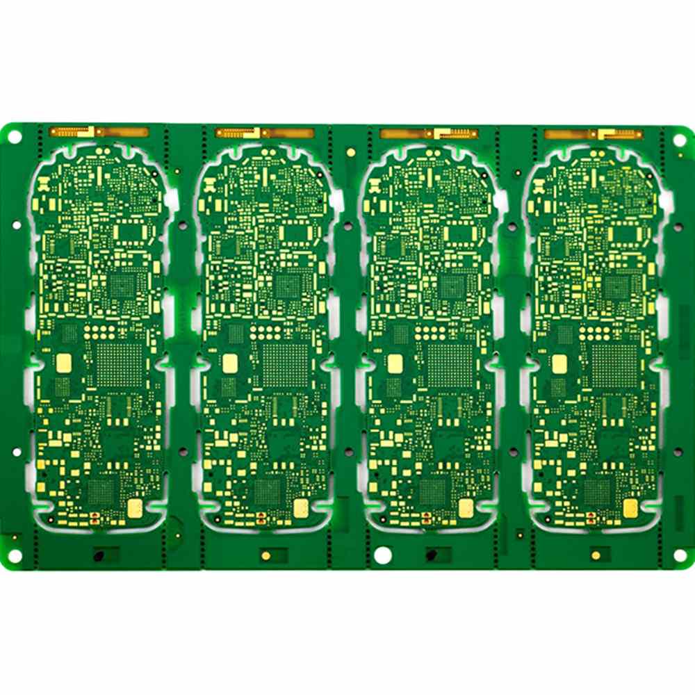
Flexible PCB (FPCB) fabrication is a specialized subset of PCB Manufacturing that enables bendable, conformable electronics—critical for applications like wearable devices, automotive wiring harnesses, and medical endoscopes. Unlike rigid PCBs, which rely on inflexible FR4 substrates, FPCBs use pliable materials (e.g., polyimide) and unique manufacturing processes to balance mechanical flexibility with electrical performance. The complexity of FPCB fabrication lies in navigating tradeoffs: maintaining trace integrity during repeated bending, ensuring uniform adhesion between layers, and preventing material degradation under environmental stress.
ShwayPCB’s PCB manufacturing services include end-to-end FPCB fabrication, from material selection to final testing, supporting designs for consumer, medical, and automotive industries. This guide breaks down the complex workflow of FPCB fabrication, explains key technical challenges and solutions, and highlights how specialized processes unlock the potential of bendable electronics.
1. Core Materials: The Foundation of Flexible PCB Fabrication
FPCB performance begins with material selection—each component must be engineered for flexibility, durability, and electrical stability. Unlike rigid PCBs, which use standard FR4, FPCBs rely on three specialized materials:
1.1 Substrates: Flexible Polymers for Bendability
The substrate is the most critical material, determining the FPCB’s flexibility, temperature range, and chemical resistance:
- Polyimide (PI): The industry standard for FPCBs, offering:
- Temperature resistance: -269°C to +400°C (continuous operation up to +200°C).
- Mechanical durability: Withstands 100k+ bend cycles (1mm radius) without cracking.
- Electrical insulation: Dielectric strength ≥40 kV/mm, suitable for high-voltage applications (e.g., automotive battery cables).
- Limitation: Higher cost than rigid FR4 (3–4x more expensive), but necessary for most flexible designs.
- Polyester (PET): A lower-cost alternative for low-stress applications (e.g., LED strips), with:
- Temperature range: -40°C to +120°C (limited to consumer electronics).
- Bend cycles: 10k+ (5mm radius) – less durable than PI.
- Liquid Crystal Polymer (LCP): For high-frequency FPCBs (e.g., 5G mmWave), LCP offers low dielectric loss (Df=0.002 at 10 GHz) and excellent dimensional stability—critical for RF signal integrity.
1.2 Conductive Layers: Thin Copper for Flexibility
FPCBs use ultra-thin copper foils to maintain flexibility while ensuring conductivity:
- Electrodeposited (ED) Copper: 9–18μm thickness (vs. 35μm for rigid PCBs), ideal for dynamic bending (e.g., smartwatch hinges). ED copper adheres well to polyimide but has lower tensile strength than rolled copper.
- Rolled Copper: 12–35μm thickness, with higher ductility (20% elongation vs. 10% for ED copper). Used for static bending (e.g., medical endoscope probes) where trace integrity under stress is critical.
1.3 Adhesives: Bonding Layers Without Compromising Flexibility
Adhesives connect substrate, copper, and coverlay (protective layer) in FPCBs. Traditional rigid PCB adhesives are too brittle—FPCBs require:
- Acrylic Adhesives: Flexible, low-cost, and compatible with most substrates. Used for consumer FPCBs (e.g., smartphone flex cables).
- Epoxy Adhesives: High-temperature resistance (+200°C) and chemical stability. Ideal for automotive/industrial FPCBs exposed to oils or solvents.
- Adhesive-Less Lamination: For high-reliability designs (e.g., aerospace), copper is directly bonded to polyimide without adhesive—eliminating delamination risks but increasing fabrication complexity.
2. The Step-by-Step Workflow of Flexible PCB Fabrication
FPCB fabrication involves 8 sequential stages, each with specialized equipment and quality controls to address the unique challenges of flexible materials:
2.1 Substrate Preparation & Copper Lamination
- Cleaning: Polyimide substrates are ultrasonic-cleaned (alkaline solution) to remove dust and oil—critical for copper adhesion. Even minor contamination causes delamination during bending.
- Lamination: Copper foil is bonded to the substrate using heat (180–220°C) and pressure (10–20 psi). For adhesive-less designs, plasma treatment of the polyimide surface enhances copper bonding.
- Quality Check: Peel strength testing (≥0.8 N/mm for PI-copper) ensures the bond withstands bending. ShwayPCB rejects batches with peel strength <0.6 N/mm to prevent field failures.
2.2 Circuit Pattern Transfer (Photolithography)
- Photoresist Coating: A thin layer of flexible photoresist (liquid or dry film) is applied to the copper surface. Dry film is preferred for FPCBs, as it conforms to the substrate without cracking.
- UV Exposure: A stencil with the circuit pattern is aligned over the photoresist, and UV light (365nm) hardens the exposed areas. FPCBs require tighter alignment tolerance (±0.01mm) than rigid PCBs, as misaligned traces are more likely to short during bending.
- Development: Unhardened photoresist is removed with a developer solution (sodium carbonate), leaving a protective mask over the copper traces.
2.3 Etching: Creating Flexible Traces
- Etchant Selection: FPCBs use cupric chloride (lower etch rate) instead of ferric chloride to avoid over-etching thin copper (9–18μm). The etch rate is controlled to ±5% to maintain trace width tolerance (±0.005mm for fine-pitch designs).
- Undercut Control: Plasma etching is used for traces ≤0.1mm to minimize undercut (≤0.003mm). Undercut weakens traces, causing them to break during bending.
- Stripping: Remaining photoresist is stripped with alkaline solutions (sodium hydroxide), revealing the copper traces.
2.4 Coverlay Application: Protecting Flexible Traces
Coverlay is a thin polyimide or PET layer that insulates traces and prevents mechanical damage—critical for FPCB durability:
- Cutting: Coverlay is laser-cut to match the FPCB shape, with openings for component pads or connectors. Laser cutting ensures precision (±0.005mm) and avoids fraying the flexible material.
- Lamination: Coverlay is bonded to the FPCB using heat (160–180°C) and pressure (5–10 psi). For high-reliability designs, a second lamination cycle ensures no air bubbles (voids <0.1mm diameter).
2.5 Drilling & Plating: Enabling Layer Interconnects
FPCBs use microvias (≤0.2mm) to connect layers, as traditional through-holes would weaken the flexible structure:
- Laser Drilling: UV lasers create microvias with ±0.002mm placement accuracy. Mechanical drilling is avoided, as it causes substrate fraying.
- Desmearing: Plasma treatment removes resin smears from via walls—critical for uniform plating. FPCBs are more prone to smearing than rigid PCBs, as polyimide melts at lower temperatures during drilling.
- Electroless Nickel-Immersion Gold (ENIG) Plating: Vias are plated with 2–3μm nickel and 0.1μm gold to ensure conductivity and corrosion resistance. Thick plating is avoided, as it reduces flexibility.
2.6 Flexibility Testing: Validating Bend Performance
Unlike rigid PCBs, FPCBs require specialized mechanical testing to ensure durability:
- Dynamic Bending Test: FPCBs are bent back and forth at a fixed radius (1–5mm) for 10k–100k cycles, with electrical continuity monitored in real time. A 10% drop in continuity indicates failure.
- Static Bending Test: FPCBs are held at a fixed bend radius (0.5–2mm) for 1,000 hours, checking for trace cracking or delamination.
- Tensile Strength Test: Measuring the force required to stretch the FPCB (≥50 MPa for PI-based designs) to ensure it withstands installation stress.
2.7 SMT Assembly: Precision Placement on Flexible Substrates
FPCBs require specialized SMT equipment to avoid damaging the flexible substrate:
- Vacuum Hold-Down: SMT machines use vacuum tables to secure the FPCB during placement, preventing warpage.
- Low-Temperature Reflow: FPCBs use lead-free solder with a lower melting point (217°C vs. 250°C for rigid PCBs) to avoid substrate deformation.
- X-Ray Inspection: 3D X-ray verifies BGA solder joints (voids <5%)—critical, as FPCB flexing can exacerbate joint failures.
2.8 Final Inspection & Packaging
- AOI (Automated Optical Inspection): 5MP cameras check for trace defects (e.g., micro-cracks, missing coverlay) that could fail during bending.
- Electrical Testing: Flying probe testers (avoiding bed-of-nails fixtures that damage FPCBs) verify continuity, insulation resistance, and impedance.
- Packaging: FPCBs are rolled or folded (per design specifications) and packaged in anti-static materials to prevent electrostatic discharge (ESD) damage—more critical for FPCBs than rigid PCBs, as thin traces are more sensitive to ESD.
3. Key Challenges in Flexible PCB Fabrication (and How to Overcome Them)
FPCB fabrication is far more complex than rigid PCB manufacturing, with three primary challenges that require specialized solutions:
3.1 Delamination: Preventing Layer Separation
Delamination (separation of substrate, copper, or coverlay) is the most common FPCB failure. Causes include:
- Poor adhesive bonding (contaminated substrates).
- Overheating during reflow (softening polyimide).
- Repeated bending (stress at adhesive interfaces).
Solutions:
- Ultrasonic cleaning of substrates before lamination.
- Using high-temperature adhesives (+200°C) for automotive/industrial FPCBs.
- Adhesive-less lamination for high-reliability designs (e.g., aerospace).
3.2 Trace Cracking: Maintaining Conductivity Under Bending
Thin FPCB traces (≤0.1mm) are prone to cracking during bending, especially at via connections. Solutions:
- Using rolled copper (higher ductility) for dynamic bending applications.
- Rounding trace corners (0.1mm radius) to reduce stress concentration.
- Adding "stress relief" loops in traces (e.g., serpentine patterns) for areas with high bend cycles (e.g., smartwatch hinges).
3.3 Dimensional Stability: Avoiding Warpage
Polyimide substrates expand/contract with temperature changes, causing trace misalignment. Solutions:
- Using LCP or high-grade polyimide (low CTE: 10–15 ppm/°C) for high-frequency FPCBs.
- Pre-conditioning substrates (thermal cycling before fabrication) to stabilize dimensions.
- Laser cutting coverlay and substrates with ±0.005mm accuracy to match trace positions.
4. FAQ: Flexible PCB Fabrication
1. How does flexible PCB fabrication cost compare to rigid PCB manufacturing?
FPCB fabrication costs 3–5x more than rigid PCB manufacturing, due to:
- Specialized materials (polyimide, rolled copper: 3–4x cost of FR4).
- Laser drilling and adhesive-less lamination (equipment costs 2–3x more than rigid PCB tools).
- Longer lead times (5–7 days for FPCB prototypes vs. 3–5 days for rigid).
However, FPCBs reduce system costs by eliminating wiring harnesses (e.g., automotive FPCBs replace 10+ wires with one flex cable, cutting assembly costs by 30%).
2. What is the maximum number of layers in a flexible PCB?
Most FPCBs are 1–4 layers, but advanced designs (e.g., aerospace wiring) can reach 8 layers. Layer count is limited by:
- Flexibility: 8-layer FPCBs have a minimum bend radius of 5mm (vs. 1mm for 1-layer).
- Manufacturing complexity: Multi-layer FPCBs require precise alignment (±0.005mm) and adhesive-less lamination to avoid delamination.
ShwayPCB has fabricated 6-layer FPCBs for medical endoscopes, balancing layer count with bendability.
3. Can flexible PCBs be used in high-temperature environments (e.g., automotive underhood)?
Yes—with high-grade polyimide substrates (Tg≥250°C) and epoxy adhesives. Key considerations:
- Temperature range: PI-based FPCBs operate reliably at -40°C to +150°C (continuous) and +200°C (short-term).
- Thermal cycling: 1,000 cycles (-40°C to +150°C) with no delamination or trace cracking.
- Chemical resistance: Epoxy adhesives resist automotive oils and coolants (per ISO 1879).
ShwayPCB’s automotive FPCBs meet IATF 16949 standards for underhood use.
4. How do you test the flexibility of a finished FPCB?
We use two industry-standard tests:
- ISTA 3A Bending Test: 100k bend cycles at 1mm radius, monitoring continuity (≤1Ω resistance change).
- IEC 60068-2-48 Test: Static bending at 0.5mm radius for 1,000 hours, checking for trace cracking via AOI.
For medical FPCBs, we add biocompatibility testing (USP Class VI) to ensure no cytotoxicity.
5. Can flexible PCBs integrate components like BGAs or connectors?
Yes—with specialized SMT processes:
- BGAs: 0.5mm-pitch BGAs are compatible with FPCBs, using low-temperature solder (217°C) and underfill epoxy to reinforce joints against bending.
- Connectors: Thru-hole connectors are avoided (they weaken flexibility); instead, surface-mount connectors (e.g., board-to-board flex connectors) are used.
ShwayPCB has integrated 0.4mm-pitch BGAs into FPCBs for 5G wearable devices, achieving 99.7% placement accuracy.
5. Conclusion
Flexible PCB fabrication is a complex, precision-driven process that unlocks the potential of bendable electronics—from wearable medical devices to automotive wiring harnesses. Its success depends on specialized materials (polyimide, rolled copper), unique manufacturing techniques (laser drilling, adhesive-less lamination), and rigorous testing to ensure durability under bending and environmental stress. While more costly than rigid PCB manufacturing, FPCBs reduce system complexity, weight, and assembly costs—making them indispensable for modern, miniaturized electronics.
ShwayPCB’s PCB manufacturing services include custom flexible PCB fabrication, with expertise in material selection, process optimization, and compliance with industry standards (ISO 13485, IATF 16949). Our team works with you to balance flexibility, performance, and cost—whether your project is a consumer wearable or a mission-critical aerospace flex cable.
To discuss your flexible PCB project, request a design review, or get a customized quote for PCB Manufacturing, contact ShwayPCB at yuan@shwaypcb.com. For detailed specs on our FPCB capabilities—including material options, layer counts, and testing protocols—visit our dedicated PCB manufacturing services page.

Copyright © 2005-2025 ShwayPCB : PCB Fabrication and Assembly Manufacturer. All Rights Reserved. POWERED BY UEESHOP


Copyright © 2005-2025 ShwayPCB : PCB Fabrication and Assembly Manufacturer. All Rights Reserved. POWERED BY UEESHOP