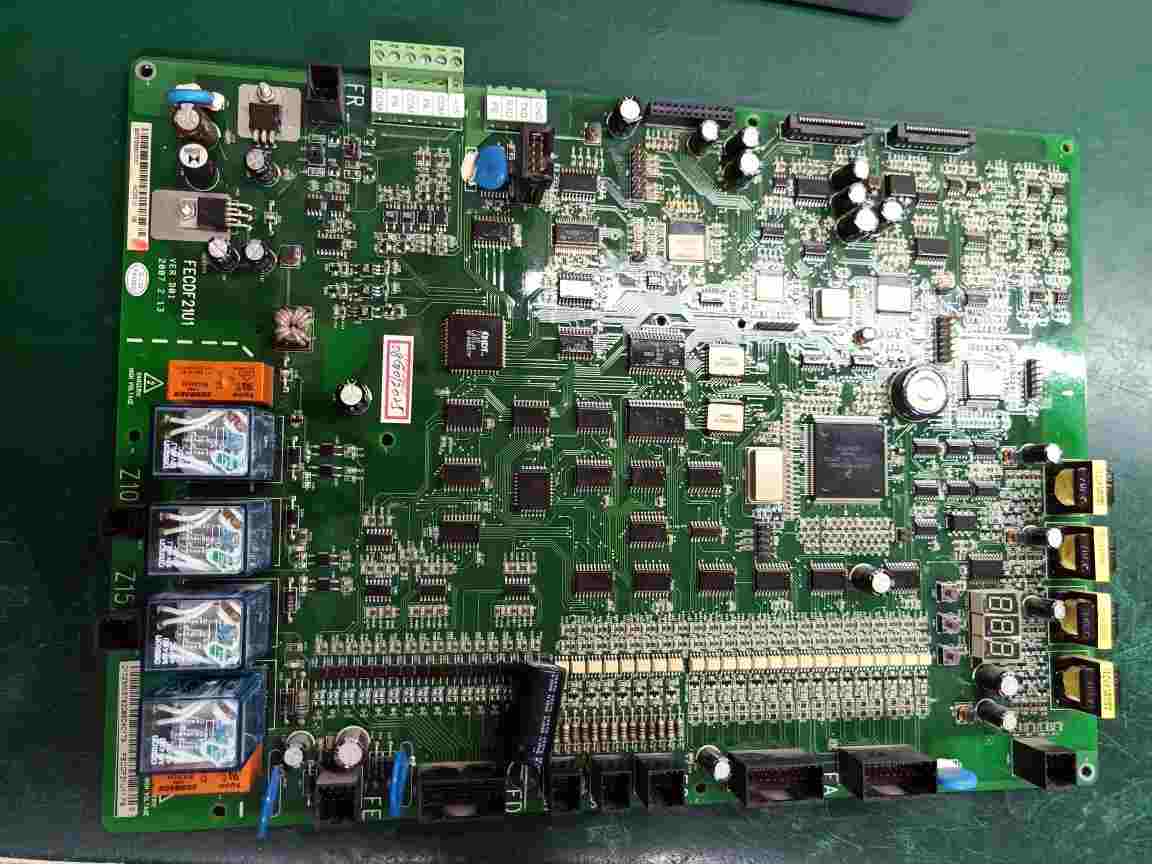
Secrets to Quality Assurance in Low-Cost PCB Manufacturing in China
Secrets to Quality Assurance in Low-Cost PCB Manufacturing in China
Amidst the fierce competition in the global electronics manufacturing industry, China has consistently maintained a dominant position in the global market with its low-cost, high-quality PCB (Printed Circuit Board) manufacturing capabilities. Data indicates that by 2025, China's PCB output value will account for over 55% of the global market share, with a year-on-year growth of 18% in exports of low-cost PCBs. Behind this achievement lies a precise balance between cost and quality achieved by Chinese manufacturers through technological innovation, process optimization, and a rigorous quality control system. This article will delve into the secrets to quality assurance in low-cost PCB manufacturing in China from four key dimensions: material selection, design optimization, process control, and quality inspection.
1. Material Selection: Dual Optimization of Cost-Effectiveness and Performance
1.1 Substrate Substitution Strategy
Chinese manufacturers employ a "tiered material selection" strategy, using modified epoxy resin copper-clad laminates in non-critical areas as an alternative to traditional FR-4 materials. This approach reduces costs by 15% while maintaining stable electrical performance. For instance, in simple control circuits like LED driver boards, a 2-layer board design combined with modified epoxy resin substrates can reduce costs by 40%. Moreover, by optimizing wiring layouts, a 4-layer board can replace a 6-layer board to achieve the same functionality.
1.2 Precise Copper Foil Thickness Matching
Chinese manufacturers adopt differentiated copper foil thickness designs based on circuit requirements: 1oz copper foil is used in signal layers to reduce material costs, while 2oz copper foil is employed in power layers to ensure high current carrying capacity. A manufacturer in Shenzhen achieved a 12% savings in copper material costs for server motherboard manufacturing through this strategy, while keeping power layer voltage drops within 0.5%.
1.3 Application of Environmentally Friendly Materials
To comply with the EU's RoHS directive, Chinese manufacturers widely adopt lead-free solder and REACH-compliant solder mask inks. For example, a factory in Jiangsu introduced water-based solder mask inks, which not only reduced VOC emissions but also improved the uniformity of solder mask layer thickness by 20%, reducing the defect rate to below 0.3%.
2. Design Optimization: Cost and Quality Control from the Source
2.1 Simplified Layer Design
Through optimized wiring strategies, Chinese designers can reduce layer counts while minimizing crosstalk. For instance, a 4-layer structure of "signal layer-ground layer-power layer-signal layer" was adopted for a communication device PCB, replacing a traditional 6-layer design. This reduced costs by 28% and met the signal integrity requirements for 5G base stations, as verified by electromagnetic simulations.
2.2 Differential Pair Wiring Specifications
Chinese manufacturers strictly adhere to equal-length and equal-spacing wiring principles for high-speed signal transmission. For example, the differential pair length error in a USB 3.0 interface PCB was controlled within ±5 mils, with impedance stability maintained at 90Ω ± 10%. The Time Domain Reflectometry (TDR) test pass rate reached 99.7%.
2.3 Application of DFM (Design for Manufacturability)
Chinese designers utilize CAD software for Design Rule Checks (DRC) and Electrical Rule Checks (ERC) to preemptively mitigate production risks. For instance, by optimizing component spacing (≥0.3mm) and pad sizes in a consumer electronics PCB, the Surface Mount Technology (SMT) assembly yield increased from 92% to 98.5%, reducing rework costs by 40%.
3. Process Control: Precision Manufacturing and Efficiency Enhancement
3.1 Symmetrical Lamination Management
In multilayer board production, Chinese manufacturers ensure uniform lamination stress through "even-layer design + prepreg thickness control." For example, an 8-layer HDI board using 0.1mm prepreg achieved layer deviation within ±2μm and warpage ≤0.5%, well below the IPC standard requirement of 0.75%.
3.2 Laser Drilling and Copper Deposition Technologies
To enhance the yield of High-Density Interconnect (HDI) boards, Chinese manufacturers have introduced CO₂ laser drilling equipment, achieving hole diameter precision of ±3μm. Combined with chemical copper deposition processes, the uniformity of hole wall copper thickness has improved to ±0.5μm, reducing microvia conduction resistance fluctuations to within 5%.
3.3 Reflow Soldering Temperature Profile Optimization
For lead-free soldering processes, Chinese manufacturers have developed a "three-stage" temperature profile: a preheat zone with a heating rate ≤2℃/s, a peak temperature of 245℃ ± 3℃, and a forced air cooling zone in the cooling phase. A automotive electronics PCB achieved a BGA solder joint void rate reduction from 15% to 3% through this process, meeting the AEC-Q100 standard.
4. Quality Inspection: Full-Process Control and Data-Driven Management
4.1 Comprehensive AOI (Automated Optical Inspection)
Chinese manufacturers deploy AOI equipment at critical process stages to achieve 100% inspection of circuits, solder joints, and silk screens. For example, an AOI system equipped with 12-megapixel cameras in a factory can identify 0.1mm line width defects at a speed of 0.8㎡/min, with a false negative rate below 0.01%.
4.2 X-Ray Inspection for Inner Layer Defects
For multilayer boards, Chinese manufacturers utilize X-Ray equipment to detect inner layer shorts, opens, and hole misregistration. A server PCB achieved an inner layer defect detection rate increase from 75% to 98% through X-Ray scanning, preventing batch scrap.
4.3 Reliability Testing System
Chinese manufacturers have established a testing system covering high-temperature/high-humidity (85℃/85%RH/96h), thermal shock (-55℃~125℃/1000 cycles), and vibration (5G/20Hz~2000Hz) tests. An industrial control PCB verified through this system achieved a Mean Time Between Failures (MTBF) of 100,000 hours, far exceeding the customer's requirement of 50,000 hours.
5. Core Advantages of Chinese PCB Manufacturing
5.1 Industrial Chain Synergy
China boasts the world's most complete PCB industrial chain, with a local procurement rate exceeding 85% for copper foil, fiberglass cloth, and specialized equipment. For instance, a manufacturer in Shenzhen collaborated with an upstream copper foil supplier to develop 12μm ultra-thin copper foil, reducing costs for high-frequency boards by 20% while decreasing signal loss by 0.5dB/inch.
5.2 Smart Manufacturing Upgrades
By introducing Manufacturing Execution Systems (MES) and AI visual inspection, Chinese manufacturers have achieved real-time production data collection and process optimization. An AI system in a factory can automatically identify over 200 defect types, with inspection efficiency increased by 5 times compared to manual methods and a false positive rate reduced from 8% to 0.5%.
5.3 Rapid Response Capabilities
Chinese manufacturers have established an agile delivery system of "72-hour prototyping + 5-day mass production" to meet urgent customer demands. A consumer electronics brand shortened its new product launch cycle from 18 months to 9 months through collaboration with Chinese manufacturers, increasing market share by 12%.
6. Case Study: Quality Control Practices in a 5G Base Station PCB
6.1 Design Phase
A 6-layer board structure was adopted, with L2/L5 as ground layers and L3/L4 as power layers. Electromagnetic simulations using HFSS optimized signal integrity, ensuring insertion loss ≤3dB/100mm for 5G high-frequency signals (24.25GHz~52.6GHz).
6.2 Production Phase
- Lamination Process: 0.08mm prepreg was used, achieving layer deviation ≤1.5μm and warpage ≤0.3%.
- Drilling Process: UV laser drilling achieved hole diameter precision of ±2μm and hole wall roughness Ra ≤1.5μm.
- Surface Finish: Electroless Nickel Immersion Gold (ENIG) process was applied, with nickel layer thickness 3~6μm and gold layer thickness 0.05~0.1μm, meeting low-loss requirements for high-frequency signals.
6.3 Inspection Phase
- AOI Inspection: Identified 0.08mm line width defects at a speed of 1.2㎡/min.
- Network Analyzer Testing: Verified impedance control accuracy (50Ω ± 5%) and insertion loss fluctuation range ≤0.2dB.
- Environmental Testing: Passed -40℃~85℃/1000-cycle thermal shock testing, with no solder joint cracking or detachment.
This case demonstrates that Chinese manufacturers can achieve mass production of high-end 5G PCBs at low costs through refined process control and rigorous inspection, with a yield rate of 99.2% and a customer complaint rate below 0.1%.
Conclusion
The quality assurance in low-cost PCB manufacturing in China stems from the deep integration of material science, precision processes, and intelligent inspection. Through a four-pronged quality control system encompassing "design-materials-processes-inspection," Chinese manufacturers not only meet global customers'极致 (ultimate) pursuit of cost-effectiveness but also achieve technological breakthroughs in high-end fields such as 5G and automotive electronics. As AI, IoT, and other technologies continue to advance, Chinese PCB manufacturing will lead global industry upgrades.
Contact Email: yuan@shwaypcb.com
Website: https://fr4pcb.tech/