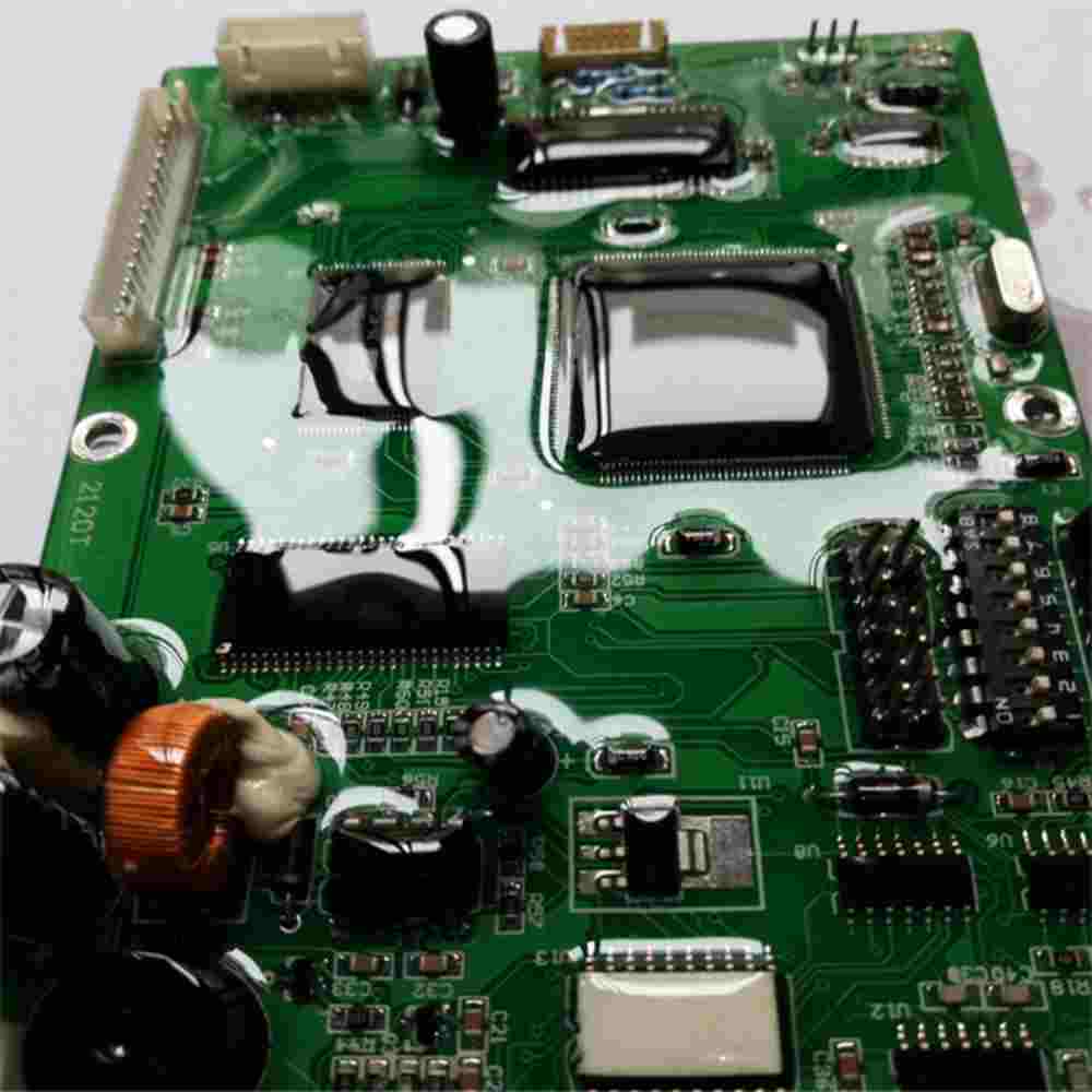
Rapid PCB Manufacturing: Decoding the 5 Core Processes - A Case Study of ShwayPCB's Turnkey PCB Assembly Model
Rapid PCB Manufacturing: Decoding the 5 Core Processes - A Case Study of ShwayPCB's Turnkey PCB Assembly Model
In the electronics manufacturing sector, rapid PCB manufacturing (Quick Turn PCB Assembly) has emerged as a cornerstone for shortening product time-to-market and mitigating R&D risks. According to Prismark data, the global PCB market reached $78 billion in 2023, with China accounting for over 53% of production. Demand for fast-turnaround services is growing at an annual rate of 15%. This article uses ShwayPCB's Turnkey PCB Assembly model as a case study to dissect the five core processes behind rapid PCB manufacturing, leveraging China's PCB Assembly industrial strengths to demonstrate how 48-hour expedited delivery is achieved.
1. Technological Foundation: Optimized Application of FR-4 Materials
FR-4 (glass-fiber-reinforced epoxy resin) remains the dominant substrate for rapid PCB manufacturing, accounting for 35-40% of material costs. ShwayPCB achieves rapid responsiveness through:
1.1 Standardized Material Preprocessing
- Inventory Management: A dynamic stocking model covers FR-4板材 (laminates) with thicknesses ranging from 0.2mm to 3.2mm, enabling 24-hour material dispatch.
- Preprocessing Workflow: Plasma cleaning removes surface oxidation from copper foils, boosting adhesion to substrates to 1.2N/mm (industry standard: 0.8N/mm) and reducing downstream defects.
1.2 Rapid Adaptation to High-Frequency FR-4
For 5G, millimeter-wave radar, and other high-frequency applications, ShwayPCB has developed a quick material-switching solution:
- Dielectric Constant Control: By adjusting glass fabric types (e.g., NE-Glass) and resin content, the dielectric constant (DK) is stabilized at 3.8-4.2 (10GHz) with ±0.1 variability.
- Loss Tangent Optimization: Low-loss resin systems (Df ≤ 0.008) support PCIe 5.0 and other high-speed signaling standards.
Case Study: A telecommunications firm required 28GHz-compatible PCB prototypes within 72 hours. ShwayPCB leveraged its pre-stocked high-frequency FR-4 inventory and laser direct imaging (LDI) technology to compress the traditional 5-day process into 48 hours.
2. Core Process 1: Laser Direct Imaging (LDI) – Enabling Micron-Level Precision at Speed
LDI technology is a game-changer for rapid PCB manufacturing, achieving ±10μm accuracy—three times better than conventional exposure methods.
2.1 Advantages of LDI
- Filmless Design: Direct Gerber file processing eliminates the 4-hour phototool fabrication and storage costs.
- Dynamic Compensation: Machine vision systems correct substrate warpage in real time, aligning multilayer boards within ±15μm.
- Multi-Wavelength Adaptability: 355nm UV lasers handle both inner-layer circuitry and solder mask layers, reducing per-panel processing time to 8 minutes.
2.2 ShwayPCB's LDI Applications
- HDI Board Production: For an AI chipmaker’s 12-layer HDI boards with 0.1mm blind vias and 0.075mm trace widths, LDI achieved a 99.2% first-pass yield.
- Rapid Design Revisions: When clients modify designs, LDI enables new data loading and first-article production within 2 hours—80% faster than traditional methods.
3. Core Process 2: Vacuum Lamination – Revolutionizing Multilayer PCB Efficiency
Multilayer lamination is a bottleneck in PCB production, with conventional hydraulic presses requiring 4-6 hours. **ShwayPCB’s vacuum lamination technology cuts this to 90 minutes.
3.1 Vacuum Lamination Principles
- Pressure Control: Servo-hydraulic systems maintain ±0.5MPa uniformity (vs. ±2MPa in traditional methods).
- Temperature Gradients: A three-stage heating profile (80°C → 150°C → 180°C) prevents interlayer delamination between copper foils and resin.
- Vacuum Environment: Maintaining 10⁻² mbar pressure during lamination eliminates air bubbles, boosting interlayer adhesion to 2.5N/mm.
3.2 Rapid Lamination Solutions
- Pre-Stacking: Inner-layer boards, prepreg (PP) sheets, and copper foils are pre-assembled to reduce on-site setup time.
- Parallel Processing: Eight vacuum presses enable simultaneous production of boards with varying layer counts, achieving a daily output of 2,000㎡.
Performance Comparison:
| Process Type | Lamination Time | Interlayer Adhesion | Yield Rate |
|---|---|---|---|
| Conventional Hydraulic Press | 6 hours | 1.8N/mm | 92% |
| Vacuum Lamination | 1.5 hours | 2.5N/mm | 98.5% |
4. Core Process 3: Selective Soldering – Accelerating THT Component Assembly
Despite SMT’s dominance, through-hole technology (THT) components remain a bottleneck. **ShwayPCB’s selective soldering technology reduces THT assembly time from 30 minutes/board (manual) to 5 minutes/board.
4.1 Technical Principles
- Localized Heating: Electromagnetically heated nozzles melt solder only at target pads, avoiding thermal stress on adjacent SMT components.
- Nitrogen Protection: A 99.99% nitrogen atmosphere cuts oxidation rates from 15% to 2%, improving solder joint reliability.
- Vision-Guided Positioning: Dual cameras (0.01mm resolution) achieve 0.05mm pin-to-pad alignment accuracy.
4.2 Rapid Assembly Case Studies
- Connector Soldering: For an industrial control board with 0.5mm-pitch connectors, selective soldering achieved a 99.7% first-pass yield—12x faster than manual methods.
- Mixed-Technology Boards: The system programs welding sequences to combine SMT (0201 components) and THT (high-power resistors) without thermal damage.
5. Core Process 4: Automated Optical Inspection (AOI) – Closing the Quality Loop at Speed
AOI is critical for rapid PCB manufacturing. ShwayPCB enhances efficiency through:
5.1 Multispectral Inspection
- Visible + Infrared Light: Simultaneously detects shorts (visible) and inner-layer voids (infrared), covering defects ≥0.05mm.
- 3D Profilometry: Laser triangulation measures solder joint height (±2μm accuracy) to identify cold solder joints.
5.2 Real-Time Feedback Mechanisms
- 5G Data Transmission: AOI results sync with the MES system in real time, triggering automated rework instructions.
- AI-Powered Defect Classification: Deep learning models reduce false rejection rates from 15% to 3%, minimizing manual review time.
Case Study: In a medical device PCB project, AOI inspected 1,000 solder joints in 2 hours, generating a report with defect locations, types, and repair recommendations—cutting rework cycles by 60%.
6. Turnkey PCB Assembly Model: Industrial Synergy for Rapid Manufacturing
**ShwayPCB’s Turnkey model integrates PCB Manufacturing, PCB Assembly, and supply chain management to accelerate end-to-end delivery.
6.1 One-Stop Service Advantages
- Concurrent Engineering: Element procurement (BOM analysis + alternative part recommendations) begins during PCB fabrication, slashing serial workflow times from 15 days to 5.
- Smart Scheduling: The ERP system dynamically prioritizes Quick Turn orders for immediate production line entry.
6.2 China’s Supply Chain Strengths
- Localized Sourcing: JIT (Just-in-Time) partnerships with suppliers like Shengyi Technology and Nanya Circuit ensure rapid delivery of critical materials (e.g., FR-4, copper foils), with inventory turnover reaching 12x/year.
- Technical Collaboration: Joint R&D with Huawei and ZTE has reduced 5G PCB development cycles from 18 months to 9.
Performance Metrics:
- Delivery Speed: Average 48-hour turnaround for standard Quick Turn orders (double-sided boards)—40% faster than industry averages.
- Cost Efficiency: Automation and scale reduce unit PCB costs by 35-50% versus Western manufacturers.
7. The Future of PCB Assembly in China
As AI, IoT, and electric vehicles surge, rapid PCB manufacturing will evolve toward:
7.1 Smart Manufacturing
- Digital Twins: Virtual production line modeling optimizes parameters in real time, reducing prototyping iterations.
- Predictive Maintenance: Sensor networks monitor equipment health, cutting downtime by 50%.
7.2 Material Innovation
- Low-Loss FR-4: Materials with Df ≤ 0.005 will support 800G/1.6T optical modules.
- Embedded Components: Direct integration of resistors and capacitors into PCBs saves 30% space.
7.3 Green Manufacturing
- Lead-Free Processes: Full adoption of SAC305 (Sn-Ag-Cu) solder aligns with RoHS 3.0 standards.
- Wastewater Recycling: Ion-exchange technology enables 80% reduction in etching solution discharge.
Conclusion
Rapid PCB manufacturing is the bedrock of electronics innovation. ShwayPCB leverages LDI, vacuum lamination, selective soldering, and other core processes—combined with a Turnkey model and China’s industrial ecosystem—to deliver 48-hour expedited services. Whether for startups validating prototypes or enterprises scaling production, fast, reliable, and cost-effective PCB solutions are now critical to market leadership.
Contact Email: yuan@shwaypcb.com
Website: https://fr4pcb.tech/