PCB Assembly Full Process: In-Depth Technical Analysis from Design to Mass Production
PCB Assembly Full Process: In-Depth Technical Analysis from Design to Mass Production
In the electronics manufacturing industry, PCB (Printed Circuit Board) assembly serves as the core link connecting electronic design to end products. With the rapid development of fields such as 5G, artificial intelligence, and new energy vehicles, PCB assembly technology is evolving toward high density, high reliability, and rapid delivery. Based on the technical practices of ShwayPCB, this article systematically analyzes the entire process from design to mass production in conjunction with the Turnkey PCB Assembly model, while exploring the technical advantages of Quick Turn PCB Assembly and the PCB Assembly China industry.
1. PCB Design: Transformation from Schematic to Manufacturing Files
The quality of PCB design directly determines assembly yield and product performance. Taking FR-4 substrate (glass fiber-reinforced epoxy resin) as an example, its excellent electrical properties (dielectric constant 4.2–4.8 @ 1 GHz), mechanical strength (tensile strength 65,000 psi), and flame retardancy (UL94V-0) make it the mainstream choice for consumer electronics and communication equipment.
1.1 Key Design Considerations
- Layer Stack Structure: Multilayer PCBs require lamination with PP prepreg (Prepreg) to achieve interlayer electrical connections. For instance, an 8-layer board typically adopts a symmetric structure of "signal layer-power layer-ground layer-signal layer" to reduce signal crosstalk.
- Impedance Control: High-speed signals (e.g., PCIe 5.0, USB4) necessitate adjusting trace width, spacing, and dielectric thickness to achieve differential impedance of 85 Ω ± 10%.
- DFM (Design for Manufacturability): Designs must avoid ultra-process capabilities such as hole diameters below 0.2 mm and trace widths below 4 mil. For example, ShwayPCB's DFM inspection tool automatically identifies over 50 design violations.
1.2 Manufacturing File Output
- Gerber Files: Contain 2D graphical data for copper layers, solder mask layers, and silkscreen layers.
- Drill Files: Define through-hole and blind via positions and diameters (accuracy ±0.05 mm).
- IPC Netlist: Provides component footprints, coordinates, and BOM (Bill of Materials) information to guide automated programming for Turnkey PCB Assembly.
2. PCB Manufacturing: Precision Processing from Substrate to Bare Board
China accounts for over 60% of global PCB manufacturing capacity. Taking representative enterprises in PCB Assembly China as examples, the typical process is as follows:
2.1 Inner Layer Circuit Fabrication
- Panel Cutting: FR-4 substrates are cut to standard sizes (e.g., 500 mm × 600 mm).
- Lamination and Exposure: Circuit patterns are transferred to copper foil via dry film photolithography with a resolution of 25 μm.
- Etching and AOI Inspection: Excess copper is removed using alkaline etching solution, and automatic optical inspection (AOI) identifies line defects larger than 0.1 mm.
2.2 Lamination and Drilling
- Brown Oxide Treatment: Chemical oxidation increases copper surface roughness to enhance interlayer adhesion.
- Vacuum Lamination: Inner layers and PP prepreg are pressed into a multilayer board at 180°C and 4 MPa, with interlayer alignment accuracy ±0.05 mm.
- Laser Drilling: For HDI (High-Density Interconnect) boards, CO₂ lasers drill 0.1 mm blind vias with an aspect ratio of 1:1.
2.3 Outer Layer Circuit and Surface Finish
- Chemical Copper Deposition and Electroplating: A 0.5 μm copper layer is deposited on hole walls, then electroplated to 25 μm thickness.
- Solder Mask and Silkscreen Printing: Liquid photoimageable solder mask (e.g., Taiyo PSR-4000) with heat resistance up to 260°C/10s is applied.
- Surface Finish:
- ENIG (Electroless Nickel Immersion Gold): Thickness 3–5 μin, suitable for fine-pitch components (e.g., 0201 packages).
- OSP (Organic Solderability Preservative): Low cost but with a storage life of only 6 months.
3. PCB Assembly: Synergistic SMT and THT Processes
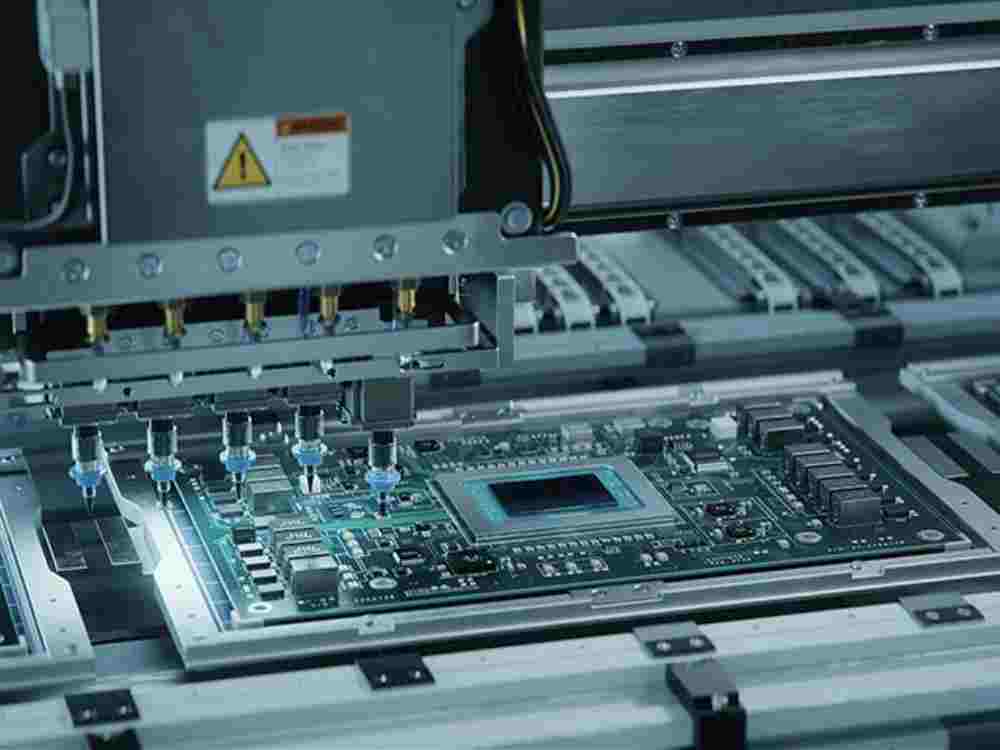
The Turnkey PCB Assembly model integrates SMT (Surface Mount Technology) and THT (Through-Hole Technology). Taking Quick Turn PCB Assembly demands as an example, the process is as follows:
3.1 SMT Assembly
- Stencil Fabrication: Laser-cut stencils are designed based on component footprints (e.g., QFN, BGA) with a thickness of 0.12–0.15 mm.
- Printing and Placement:
- Solder Paste Printing: Lead-free solder (SAC305) is printed with an accuracy of ±0.03 mm.
- High-Speed Placement: Siemens HS60 placers achieve 60,000 CPH (components per hour) with ±0.04 mm accuracy.
- Reflow Soldering: A ten-zone reflow oven implements gradient heating (150°C → 245°C → 180°C) to avoid thermal shock to components.
3.2 THT Insertion and Wave Soldering
- Selective Wave Soldering: Localized soldering is performed on through-hole components (e.g., connectors, inductors) using nozzles to minimize thermal stress.
- Manual Rework: Components with leads below 0.5 mm are manually corrected to ensure a solder joint fill rate ≥95%.
3.3 Quality Inspection and Rework
- AOI and X-Ray Inspection:
- AOI: Detects defects such as insufficient solder and bridges at speeds up to 20 cm²/s.
- X-Ray: Inspects BGA solder joints for voids and cold solder internally.
- ICT (In-Circuit Testing): Flying probe testers verify circuit connectivity with 100% test point coverage.
4. Mass Production Optimization: From NPI to Large-Scale Manufacturing
4.1 NPI (New Product Introduction) Phase
- Pilot Production Validation: 10–50 prototype boards are manufactured for HALT (Highly Accelerated Life Testing) to verify reliability under extreme temperatures (-40°C to 125°C).
- Process Optimization: Reflow oven temperature profiles and solder paste printing parameters are adjusted to improve first-pass yield from 85% to 98%.
4.2 Large-Scale Production Control
- Material Traceability System: QR codes bind BOMs, process parameters, and test data for full-process traceability.
- Automated Production Lines: AGV trolleys and robotic arms automate material handling and loading/unloading, reducing labor costs by 40%.
4.3 Advantages of China's PCB Assembly Industry
- Cost Efficiency: PCB assembly costs in China are 30%–50% lower than in Europe and the U.S., with lead times shortened to 7–10 days.
- Technical Collaboration: Enterprises like ShwayPCB collaborate with Huawei and ZTE to develop high-speed PCBs for 5G base stations with signal loss ≤0.1 dB/inch @ 28 GHz.
5. Industry Trends and ShwayPCB's Technological Innovations
5.1 Material Upgrades
- High-Frequency FR-4: Incorporating PTFE (polytetrafluoroethylene) fillers reduces dielectric loss to 0.002 @ 10 GHz, suitable for millimeter-wave radar.
- Halogen-Free Materials: Comply with RoHS 3.0 standards, achieving UL94V-0 flame retardancy without toxic smoke emissions.
5.2 Process Innovations
- SLP (Substrate-Like PCB) Technology: Modified Semi-Additive Process (mSAP) achieves 20/20 μm line/space widths for smartphone motherboards.
- Embedded Component Technology: Resistors and capacitors are embedded directly into PCBs, saving 30% space.
Conclusion
PCB assembly is the "heart" of electronics manufacturing, with its technological complexity and supply chain collaboration capabilities directly determining product competitiveness. ShwayPCB integrates design, manufacturing, and testing through the Turnkey PCB Assembly model, combining the rapid responsiveness of Quick Turn PCB Assembly to provide global customers with highly reliable PCB solutions. Whether addressing the miniaturization demands of consumer electronics or the harsh environmental requirements of industrial controls, China's PCB assembly industry is leading global electronics manufacturing upgrades through technological innovation.
Contact Email: yuan@shwaypcb.com
Website: https://fr4pcb.tech/