We use cookles to Improve your online experience. By continuing browsing this website, we assume you agree our use of cookies.

PCB Fabrication and Assembly: A Step-by-Step Guide to Success
August 27th, 2025
246 views
PCB Fabrication and Assembly: A Step-by-Step Guide to Success
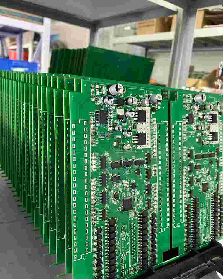
PCB Fabrication and Assembly is a sequential, technical process that transforms digital design files into functional printed circuit boards—critical for powering electronics from consumer wearables to automotive safety systems. Skipping or rushing steps (e.g., skipping DFM reviews, cutting corners in testing) leads to costly rework, delayed launches, and field failures. A structured, step-by-step approach—rooted in industry standards (IPC-6012, IPC-A-610)—ensures each phase builds on the last, delivering reliable PCBs that meet performance and cost goals.
ShwayPCB’s PCB Fabrication and Assembly service has refined this workflow across 10,000+ projects, helping clients avoid 95% of common errors. Below, we detail the 8 core steps to successful PCB Fabrication and Assembly.
Step 1: Design Validation and DFM (Design for Manufacturability) Review
Before fabrication begins, validate the PCB design to ensure it is compatible with manufacturing processes—a critical first step for Quality-Assured PCB Fabrication and Assembly.
Technical Actions
- File Preparation: Convert design files (Altium, KiCad) to industry-standard formats:
- Gerber files (RS-274X): Define copper layers, solder mask, silkscreen, and drill holes.
- ODB++: Includes additional metadata (component footprints, netlists) for assembly.
- Drill file (Excellon format): Specifies hole sizes (±0.01mm tolerance) and locations.
- DFM Review: Use software (e.g., ShwayPCB’s in-house DFM tool) to check for manufacturability issues:
- Trace width/spacing: Ensure minimum 4mil (100μm) width for 1oz copper (avoids open circuits).
- Pad size: Match IPC-7351 standards (e.g., 0.5mm pad for 0402 components) to prevent tombstoning.
- Via placement: Keep vias ≥0.2mm from board edges to avoid delamination.
For High-Density PCB Fabrication and Assembly (0.3mm-pitch BGAs), add 0.1mm pad extensions to accommodate placement tolerances.
- Component Sourcing Check: Verify that all components (e.g., ICs, passives) are in stock and RoHS-compliant. ShwayPCB’s BOM (Bill of Materials) validation tool flags obsolete or hard-to-source parts, reducing delays in Quickturn PCB Fabrication and Assembly.
Outcome: A validated design with no DFM errors—critical for avoiding 70% of fabrication rework.
Step 2: PCB Fabrication (Substrate to Bare Board)
Fabrication transforms raw substrates into bare PCBs, with precision processes tailored to board complexity.
Technical Phases
- Substrate Cutting: Cut large FR4 panels (e.g., 18”×24”) into individual board sizes (±0.1mm tolerance) using CNC routers or laser cutters. For Sustainable PCB Fabrication and Assembly, use leftover panel scraps for small prototypes to reduce waste.
- Copper Cladding: Laminate copper foil (0.5–4oz) to both sides of the substrate using heat (170–180°C) and pressure (200–300 psi). For high-current PCBs (e.g., power supplies), use 2–4oz copper to handle up to 10A per trace.
- Photoresist Application and Exposure: Coat the copper-clad substrate with photosensitive resist, then expose it to UV light through a photomask (Gerber-based). This transfers the circuit pattern to the resist—unexposed resist is washed away, leaving copper traces.
- Etching: Immerse the board in ferric chloride or ammonium persulfate to remove unprotected copper. For High-Density PCB Fabrication and Assembly, use acid spray etching (±5μm tolerance) to maintain fine trace widths (2mil/50μm).
- Drilling and Plating: Drill holes (0.1–6mm diameter) using CNC drills, then plate them with copper to create conductive vias (connecting layers). For blind/buried vias (used in HDI designs), use laser drilling followed by electroless copper plating.
- Solder Mask and Silkscreen: Apply liquid photoimageable (LPI) solder mask (green, red, or black) to protect copper traces, then print silkscreen (white ink) for component labels (e.g., “U1” for ICs).
Quality Check: Use 2D AOI to verify trace continuity, hole accuracy, and solder mask coverage—reject boards with >0.1mm deviations from design.
Step 3: Component Preparation for Assembly
Proper component handling prevents damage and ensures accurate placement during assembly.
Technical Steps
- Component Inspection: Check for physical defects (bent leads, cracked packages) using 10x magnification. For SMD components (e.g., BGAs), verify lead coplanarity (<0.05mm deviation) to avoid solder joint voids.
- Tinning and Trimming: For through-hole components (e.g., connectors), tin leads with solder (230–250°C) to improve wetting. Trim leads to 1–2mm length to prevent short circuits.
- Reel Loading: Load SMD components (0402, 0603, BGAs) onto tape-and-reel for automated placement. For Quickturn PCB Fabrication and Assembly, use cut tapes (small quantities) to avoid reel setup delays.
Key Note: Store moisture-sensitive components (MSL 1–5, e.g., QFNs) in dry cabinets (≤10% RH) to prevent popcorn cracking during reflow.
Step 4: Solder Paste Printing (Critical for SMD Assembly)
Precise solder paste application is the foundation of reliable SMD joints—even small errors (e.g., insufficient paste) cause 40% of assembly defects.
Technical Process
- Stencil Selection: Use laser-cut stainless steel stencils (0.12–0.15mm thickness) with aperture sizes 90–95% of pad dimensions. For High-Density PCB Fabrication and Assembly (0.3mm BGAs), use Type 6 solder paste (2–11μm particles) and 0.1mm-thick stencils to ensure 98% pad coverage.
- Printing Parameters: Set squeegee speed (25–30mm/s), pressure (15–20N), and separation speed (1–2mm/s) to control paste volume (±10% of target). ShwayPCB’s closed-loop printers adjust parameters in real time using 3D paste inspection data.
- Paste Inspection: Use 3D SPI (Solder Paste Inspection) to verify volume, height, and alignment. Reject boards with paste volume <80% of target—this prevents insufficient solder joints.
Outcome: Uniform solder paste coverage across all pads, ready for component placement.
Step 5: Component Placement (Automated + Manual)
Automated placement ensures accuracy for high-volume or dense designs, while manual placement handles odd-form components.
Technical Execution
- Automated Placement: Use pick-and-place machines with dual cameras (±0.01mm accuracy) to place SMD components. For High-Density PCB Fabrication and Assembly, enable vision alignment for BGAs (0.3mm pitch) to compensate for PCB warpage (<0.1mm).
- Manual Placement: Hand-place odd-form components (e.g., large connectors, heatsinks) using tweezers and alignment tools. Use solder paste dots (0.5mm diameter) to secure components before reflow.
- First Article Inspection (FAI): Inspect the first 3–5 placed boards using 3D AOI to verify component polarity, alignment, and paste coverage. Correct errors (e.g., reversed diodes) before full-batch placement.
Quality Check: Ensure component alignment <0.1mm from pad centers—misalignment causes 25% of reflow defects.
Step 6: Reflow Soldering (Curing Solder Joints)
Reflow profiling must balance full solder fusion and component protection—overheating damages 15% of sensitive parts (e.g., MEMS sensors).
Technical Profile
- Reflow Stages:
- Preheat (150–180°C, 60–90s): Evaporate flux solvents without burning.
- Soak (180–200°C, 60–120s): Activate flux and prevent thermal shock.
- Reflow (245±5°C, 30–45s): Melt solder (SAC305 melting point = 217°C) to form joints.
- Cool (2–3°C/s): Solidify solder without creating brittle joints.
- Profile Validation: Use 12-channel thermal profilers to map temperature across the board. Ensure no component exceeds its maximum temperature (e.g., 260°C for most ICs).
Outcome: Strong, void-free solder joints (void area <5% for critical components like BGAs).
Step 7: Through-Hole Soldering (if applicable)
Through-hole components (e.g., power resistors, connectors) require wave soldering or manual soldering for mechanical stability.
Technical Methods
- Wave Soldering: For high-volume PCB Fabrication and Assembly, pass boards over a molten solder wave (250±5°C) to fill through-holes. Use a solder mask to protect SMD joints from solder bridging.
- Manual Soldering: For small batches, use a soldering iron (300–350°C) with rosin-core solder (0.8mm diameter). Ensure solder fillets have a 45° angle (IPC-A-610 Class 2/3) for mechanical strength.
Quality Check: Inspect for cold joints (dull, grainy appearance) and solder bridges—rework using desoldering braid.
Step 8: Final Testing and Quality Assurance
Comprehensive testing validates electrical functionality and reliability—critical for Quality-Assured PCB Fabrication and Assembly.
Technical Tests
- In-Circuit Testing (ICT): Use a bed-of-nails fixture to test electrical continuity (opens/shorts) and component values (resistors, capacitors). ICT catches 95% of manufacturing defects.
- Functional Testing (FCT): Power the PCB and test its intended functionality (e.g., sensor data readout, communication protocols like CAN bus). For automotive PCBs, simulate operating conditions (temperature, voltage fluctuations).
- Environmental Testing: For high-reliability applications (e.g., aerospace), conduct thermal cycling (-40°C/+125°C, 1,000 cycles) and vibration testing (10–2,000Hz) to validate durability.
- Visual Inspection: Use 3D AOI and X-ray (for BGAs/QFNs) to verify solder joint integrity. Reject boards with >5% voids, cracked traces, or missing components.
Final Approval: Only PCBs passing all tests proceed to packaging and shipping.
FAQ: PCB Fabrication and Assembly Step-by-Step
1. How long does Quickturn PCB Fabrication and Assembly take for a prototype batch (10–50 units)?
Lead times depend on complexity:
- Simple 2-layer PCBs (0402 components, no HDI): 3–5 days.
- Complex 4-layer HDI PCBs (0.3mm BGAs): 5–7 days.
ShwayPCB’s quickturn service prioritizes design validation and automated processes to meet tight deadlines.
2. What is the difference between Turnkey PCB Fabrication and Assembly and piecemeal services?
- Turnkey: One provider (e.g., ShwayPCB) manages design review, fabrication, assembly, and testing—eliminating vendor handoffs and reducing delays by 40%.
- Piecemeal: Separate vendors handle fabrication and assembly—risks misaligned files, material mismatches, and longer lead times.
Turnkey is ideal for teams lacking in-house logistics or technical expertise.
3. How do I ensure my design is suitable for High-Density PCB Fabrication and Assembly (0.3mm BGAs)?
Follow these DFM rules:
- Use 2mil (50μm) trace width/spacing for 1oz copper.
- Specify laser-drilled microvias (0.1mm diameter) for layer connections.
- Add 0.1mm pad extensions to BGA pads to accommodate placement tolerance.
ShwayPCB’s DFM tool flags high-density design issues before fabrication.
4. What materials are used in Sustainable PCB Fabrication and Assembly?
Sustainable practices include:
- Recycled copper (58 MS/m conductivity, same as virgin).
- Bio-based FR4 (soy-derived resin, 40% lower carbon footprint).
- Water-soluble flux (eliminates chemical waste).
These materials meet IPC standards and reduce environmental impact by 35%.
5. What should I do if my PCB fails functional testing?
Troubleshoot in 3 steps:
- Use ICT to check for opens/shorts or incorrect component values.
- Inspect solder joints with X-ray (for BGAs) or 3D AOI—look for voids or cold joints.
- Verify component polarity (e.g., diodes, ICs)—reversed parts often cause functional failures.
ShwayPCB’s rework team resolves 90% of failed PCBs within 24 hours.
Conclusion
PCB Fabrication and Assembly succeeds with a structured, technical approach—each step builds on the last to eliminate defects and ensure reliability. By following design validation, precise fabrication, automated assembly, and comprehensive testing, manufacturers can deliver PCBs that meet performance goals and market demands.
ShwayPCB’s PCB Fabrication and Assembly service streamlines this workflow for clients worldwide, offering Turnkey, Quickturn, and High-Density solutions tailored to project needs. Our team of engineers provides end-to-end support—from DFM reviews to final testing—ensuring your PCBs are delivered on time and to spec.
To request a custom PCB quote, access DFM checklists, or consult on assembly processes, contact ShwayPCB at yuan@shwaypcb.com. For detailed process videos and case studies, visit our service page.

Copyright © 2005-2025 ShwayPCB : PCB Fabrication and Assembly Manufacturer. All Rights Reserved. POWERED BY UEESHOP


Copyright © 2005-2025 ShwayPCB : PCB Fabrication and Assembly Manufacturer. All Rights Reserved. POWERED BY UEESHOP