We use cookles to Improve your online experience. By continuing browsing this website, we assume you agree our use of cookies.

AI-Driven PCB Design Optimization: How Machine Learning Reduces DFM Issues by 50%
August 21st, 2025
290 views
AI-Driven PCB Design Optimization: How Machine Learning Reduces DFM Issues by 50%
Design for Manufacturability (DFM) issues—from suboptimal component placement to incompatible trace widths—have long been a costly bottleneck in PCB production, delaying prototypes, increasing rework, and inflating costs. For startups and enterprise manufacturers alike, these issues can add 2–4 weeks to development cycles and raise production expenses by 30–50%. However, advancements in artificial intelligence (AI) and machine learning (ML) are transforming this landscape. By analyzing millions of design-manufacturing pairs, ML algorithms can predict and prevent DFM issues in real time, cutting their occurrence by 50% or more. This guide explores how AI-driven design optimization works, its impact on prototyping timelines, and why integrating these tools with quick turn PCBA prototypes creates a powerful synergy for fast, cost-effective production.
1. How ML Algorithms Identify DFM Risks
Machine learning systems leverage vast datasets to learn patterns that human designers or traditional rule-based software might miss:
- Training on Historical Data: ML models are trained on databases of thousands of PCBs, each labeled with their DFM issues (e.g., "solder mask bridging," "insufficient clearance") and manufacturing outcomes. This allows the algorithm to recognize subtle correlations—for example, how a 0.2mm trace width on a 4-layer FR4 PCB correlates with 80% higher etch defects in high-volume production.
- Real-Time Design Scanning: As a designer places components or routes traces, the ML tool scans the layout 10–100x faster than manual checks, flagging issues like:
- Component footprints mismatched to assembly equipment capabilities
- Trace spacing that violates IPC-2221 standards for the chosen substrate
- Thermal vias positioned too far from high-power components
- Context-Aware Recommendations: Unlike static DFM checklists, ML systems provide context-specific fixes. For example, if a BGA placement risks solder bridging, the algorithm might suggest a 0.1mm offset based on data from 500+ similar designs, rather than a generic "increase spacing" advice.
A 2024 study by the PCB Designers Association found that ML-driven DFM tools reduced post-fabrication issues by 52% compared to traditional methods, with the biggest gains in complex designs (8+ layers, fine-pitch components).
2. Predictive Component Sourcing and Placement
AI optimizes not just design geometry but also component selection and placement—critical for reducing assembly delays:
- Supplier-Specific Component Validation: ML tools integrate with quick turn PCBA prototypes providers’ databases to flag components that are difficult to source or assemble in low volumes. For example, the algorithm might warn that a specific 0201 capacitor has a 3-day lead time for prototyping, suggesting a readily available 0402 alternative with similar specs.
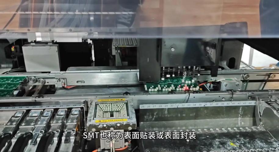
- Placement for Assembly Speed: ML analyzes pick-and-place machine capabilities (e.g., nozzle sizes, feeder types) to optimize component arrangement. Grouping similar components reduces nozzle changes, cutting assembly time by 15–20% for prototypes. For a 200-component PCB, this translates to 4–6 hours saved in production.
- Thermal and Signal Integrity Tradeoffs: Advanced models balance DFM with performance, avoiding "over-designing" to prevent manufacturability issues. For example, an algorithm might recommend a 0.3mm trace width (vs. 0.4mm) for a low-power signal, reducing material usage without compromising signal integrity—a change that saves 8% on fabrication costs.
By aligning component choices with manufacturing realities, AI ensures designs are not just functional but also production-ready from day one.
3. Integration with Quick Turn Prototyping Workflows
The true power of AI-driven design emerges when paired with rapid prototyping services:
- Seamless Data Sharing: ML design tools sync with quick turn PCBA prototypes providers’ manufacturing execution systems (MES), sharing DFM reports, component lists, and process parameters. This eliminates manual data entry errors and reduces setup time by 25–30%.
- Feedback Loops for Continuous Improvement: After prototyping, production data (e.g., defect locations, first-pass yield) is fed back into the ML model, refining its recommendations for future designs. A medical device startup using this loop saw DFM issues drop from 12 per prototype to 3 over three iterations.
- Rapid Iteration with Predictive Rework: If a prototype does require rework, AI predicts the fastest fix based on historical data. For example, it might recommend adjusting a solder paste stencil aperture instead of redesigning a component footprint, saving 1–2 days in the 48-hour prototyping window.
This integration creates a virtuous cycle: faster prototypes generate more data, which improves AI recommendations, leading to even faster, higher-quality prototypes.
4. Reducing Rework in High-Risk Applications
AI-driven optimization is particularly impactful for industries where DFM issues carry high stakes:
- Medical Devices: For Class II/III devices, ML ensures designs comply with ISO 13485 and FDA regulations while avoiding manufacturability issues. For example, algorithms flag crevices in PCB layouts that could trap bacteria (a violation of ISO 14644) and suggest smoother contours that are both sterile and easier to assemble.
- Aerospace and Defense: ML tools trained on military standards (e.g., MIL-PRF-31032) prevent DFM issues that could compromise reliability, such as insufficient trace spacing in high-vibration environments. This reduces rework rates by 60% in radar and communication PCB prototypes.
- Automotive Electronics: With strict IATF 16949 requirements, AI optimizes designs for both manufacturability and durability, ensuring PCBs withstand temperature cycling and chemical exposure without costly over-engineering.
In these sectors, the 50% reduction in DFM issues translates to fewer regulatory delays and lower liability risks, in addition to faster time-to-market.
5. Implementing AI-Driven Design: Practical Steps
Adopting ML-based DFM optimization requires careful planning but is accessible to organizations of all sizes:
- Start with a Focused Dataset: Begin by training the AI on your most common PCB types (e.g., 2–4 layer consumer electronics boards) rather than a broad range. This ensures relevant recommendations from day one.
- Integrate with Existing Tools: Choose ML plugins compatible with popular EDA software (Altium, KiCad, Mentor PADS) to avoid disrupting existing workflows. Most tools offer APIs for seamless integration.
- Collaborate with Prototyping Partners: Work with quick turn PCBA prototypes providers that share manufacturing data to enhance your AI model. Many providers offer anonymized datasets from past projects to accelerate training.
- Train Design Teams on AI Outputs: Ensure engineers understand how to interpret ML recommendations, distinguishing between critical issues (e.g., short circuits) and optional optimizations (e.g., cost-saving trace adjustments).
A survey of early AI adopters found that 78% achieved a positive ROI within 6 months, with the fastest returns in high-volume or high-complexity designs.
FAQ
Q: How accurate are ML predictions for DFM issues?
A: Leading ML tools achieve 85–90% accuracy for common issues (e.g., trace spacing, component placement). Accuracy improves with more data—organizations using quick turn PCBA prototypes to generate feedback loops often reach 95%+ accuracy within a year.
Q: Do AI-driven design tools replace human engineers?
A: No—they augment human expertise. ML handles repetitive DFM checks and data analysis, freeing engineers to focus on creative problem-solving and performance optimization.
Q: Is AI optimization only viable for large enterprises?
A: No. Cloud-based ML tools (e.g., Siemens Xcelerator, Autodesk Fusion 360) offer pay-as-you-go pricing, making them affordable for startups. Many quick turn PCBA prototypes providers also include AI DFM checks in their service at no extra cost.
Q: How much time does AI add to the design phase?
A: AI adds 5–10% to initial design time due to setup and analysis but reduces total development time by 30–40% by eliminating rework and delays.
Q: Can AI handle custom or proprietary components?
A: Yes, with proper training. Uploading data on custom components (footprints, assembly requirements) allows the ML model to include them in its recommendations, though accuracy improves with more usage data.
AI-driven PCB design optimization is reshaping how manufacturers approach DFM, turning a reactive process into a proactive one. By reducing DFM issues by 50% or more, machine learning not only cuts costs but also enables the fast, reliable prototyping that today’s market demands. When paired with quick turn PCBA prototypes, these tools create a workflow where designs move from concept to physical prototype in days, not weeks. ShwayPCB integrates AI DFM checks into its rapid prototyping services, helping startups and enterprises alike leverage machine learning for faster, higher-quality PCBs. To learn how to implement these tools for your next project, contact ShwayPCB at yuan@shwaypcb.com.

Copyright © 2005-2025 ShwayPCB : PCB Fabrication and Assembly Manufacturer. All Rights Reserved. POWERED BY UEESHOP


Copyright © 2005-2025 ShwayPCB : PCB Fabrication and Assembly Manufacturer. All Rights Reserved. POWERED BY UEESHOP