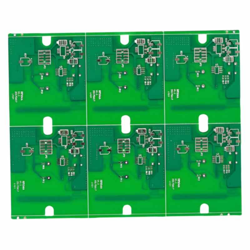
| High-Layer Count PCBs Technics Capacity |
| No. |
Item |
Description |
DataSheet |
| 1 |
Layer |
Layer |
1-98 |
| 2 |
Material |
Brand |
SY, ITEQ, KB, NanYa, Doosan, Isola, TUC, EMC, Ventec |
| 3 |
Surface treatment |
|
HASL lead-free,Immersion Gold, OSP, Immersion Tin, Immersion Silver,
Plating Gold, Plating Tin, ENEPIG |
| 4 |
Selectivity surface treatment |
|
ENIG+OSP, ENIG+G/F, Flash Gold+G/F, Immersion Silver+G/F, Immersion
Tin+G/F |
| 5 |
Solder mask color |
|
Green, Yellow, Black, Matte black, Blue, Red, White,Matte green |
| 6 |
Silkscreen color |
|
White, Yellow, Black |
| 7 |
Max board size with 2L |
mm |
2000*1500mm |
| 8 |
Max board size with 4L,6L |
mm |
1200*1000mm(Exceeding 570mm shall be reviewed) |
| 9 |
Max board size with more than 8L |
mm |
1200*1000mm(Exceeding 570mm shall be reviewed) |
| 10 |
Min board size |
mm |
0.5*1.0mm(thickness≤0.5mm), 1.0*2.0mm(thickness≥0.5mm) |
| 11 |
Min outline tolerance |
mm |
±0.05mm(Laser Routing), ±0.1mm(Mechanical Routing) |
| 12 |
PCB Board Thickness |
mm |
0.13-8mm |
| 13 |
Double side board thickness |
mm |
0.13-3.6mm |
| 14 |
4Layers board thickness |
mm |
0.30-7mm |
| 15 |
6Layers board thickness |
mm |
0.6-8mm(6L), 0.8-8mm(8L), 1.0-8mm(10L), 1.0-8mm(12L) |
| 16 |
The tolerance of board thickness |
mm |
±0.1mm(thickness≤1.0mm), ± 10%mm(thickness>1.0mm) |
| 17 |
Min Drilling hole size |
mm |
0.075-0.1mm(Laser), 0. 15mm(Mechanical) |
| 18 |
Single Max Drilling |
ww |
6.5mm(Drill Bit) |
| 19 |
Max Drilling |
ww |
50mm |
| 20 |
Min PTH tolerance |
mm |
±0.05mm, ±0.075mm |
| 21 |
Min NPTH tolerance |
mm |
±0.05mm(Limitation+0, -0.05mm or +0.05, -0mm) |
| 22 |
Min hole tolerance |
ww |
±0.075mm |
| 23 |
Max Drilling tolerance |
ww |
±0.1mm |
| 24 |
Slot hole |
mm |
0.5-6mm |
| 25 |
Min slot hole length |
mm |
1.0mm |
| 26 |
Slot hole aspect ratio |
mm |
1:2 |
| 27 |
Min slot hole tolerance |
mm |
Slot width, ±0.15mm |
| 28 |
Min slot hole tolerance |
mm |
Slot width directiont0.10, slot length direction±0.15 |
| 29 |
Countersink hole angle &size |
|
Big hole82, 90, 120degree, dia≤10mm |
| 30 |
Countersink hole angle & size |
|
PTH&NPTH, Big hole angle 130degree, The dia of the large hole is not
greater than 6.3mm |
| 31 |
Min pattern width/spacing |
mm |
0.075mm/0.075mm |
| 32 |
Pattern width tolerance |
mm |
±20um |
| 33 |
Min pad |
mm |
0.15mm |
| 34 |
FR-4 PP |
|
106, 1080, 3313, 2116, 7628 |
| 35 |
Mult press blind buried hole production |
|
Press on the same sides5 |
| 36 |
Max bore diameter of pad hole plug hole |
mm |
0.4 Multi press blind & buried hole board |
| 37 |
Min thickness of inner |
mm |
0.05(none blind buried hole), 0. 13(blind buried hole) |
| 38 |
Min inner |
mil |
3(18um base copper), 4(35um base copper), ≥3mil |
| 39 |
Inner layer treatment |
|
Brown Oxygen |
| 40 |
Min inner pattern spacing
(105um base copper, after compensation) |
mil |
5 |
| 41 |
Min inner layer pattern spacing
(140um base copper, after compensation) |
mil |
7 |
| 42 |
Min innner layer pattern spacing
(18um base copper, after compensation) |
mil |
3 |
| 43 |
Min inner layer pattern spacing
(35um base copper, after compensation) |
mil |
3.5 |
| 44 |
Min inner layer pattern spacing
(70um base copper, after compensation) |
mil |
4 |
| 45 |
Min inner layer pattern width
(105um base copper, before compensation) |
mil |
5 |
| 46 |
Min inner layer pattern width
(140um base copper, before compensation) |
mil |
7 |
| 47 |
Min inner layer pattern width
(18um base copper, before compensation) |
mil |
3 |
| 48 |
Min inner layer pattern width
(35um base copper, before compensation) |
mil |
3 |
| 49 |
Min inner layer pattern width
(70um base copper, before compensation) |
mil |
4 |
| 50 |
Min outer layer pattern spacing
(105um base copper, after compensation) |
mil |
6 |
| 51 |
Min outer layer pattern spacing
( 12, 18um base copper, after compensation) |
mil |
3.0(18um), 2.5(12um) |
| 52 |
Min outer layer pattern spacing
(140um base copper, after compensation) |
mil |
7 |
| 53 |
Min outer layer pattern spacing
(35um base copper, after compensation) |
mil |
3.5 |
| 54 |
Min outer layer pattern spacing
(70um base copper, after compensation) |
mil |
5 |
| 55 |
Min outer layer pattern width
(105um base copper, before compensation) |
mil |
8 |
| 56 |
Min outer layer pattern width
( 12, 18um base copper, before compensation) |
mil |
3.5(18um), 3(12um) |
| 57 |
Min outer layer pattern width
(140um base copper, before compensation) |
mil |
9 |
| 58 |
Min outer layer pattern width
(35um base copper, before compensation) |
mil |
4.5 |
| 59 |
Min outer layer pattern width
(70um base copper, before compensation) |
mil |
6 |
| 60 |
Min.spacing from pattern to pad, pad to pad
for outer layer(after compensation) |
mil |
3(12, 18um), 3.5(35um), 5(70um), 6(105, 140um) |
| 61 |
Min.outer pattern and spacing with blind/buried
holes plated many times(>=2times) |
mil |
3.5/3.5 (before compensation) |
| 62 |
Min distance from inner layer edge without
copper leakage |
mil |
10 |
| 63 |
Min inner layer isolation width |
mil |
8 |
| 64 |
Min inner layer isolation ring |
mil |
8(≤6layer), 10(≥8layer) |
| 65 |
Min single side width of inner pad
(none blind buried hole) |
mil |
4.5(18, 35um, Can be partial 4), 6(70um), 8(105um) |
| 66 |
Min single side width of inner pad
(laser hole) |
mil |
3 |
| 67 |
Impedance tolerance |
% |
±5Ω(<50Ω), ± 10%(≥50Ω);
≥50Ω±5%(need to evaluate when it requests), |
| 68 |
Min BGA pad diameter |
mil |
7mil |
| 69 |
Min pad diameter |
mil |
12(0.10mmMechanical or laser drilling) |
| 70 |
Min hole copper thinckness
(none blind buried hole) |
um |
average 25, min single point≥20 |
| 71 |
Min hole copper thinckness
(blind buried hole) |
um |
averager 20, min single point≥18 |
| 72 |
PP thickness(min) |
um |
0.075(only H oz base copper) |
| 73 |
ENIG: gold thickness |
um |
0.025-0.10 |
| 74 |
ENIG: nickle thickness |
um |
3-5 |
| 75 |
Immersion silver.silver thickness |
um |
0.1-0.3 |
| 76 |
Min HASL LeadFree/pure tin thickness |
um |
0.4 |
| 77 |
Gold Finger:gold thickness |
um |
0.25-1.3(The required value is the thinnest point) |
| 78 |
Gold Finger:nickle thickness |
um |
3-5 |
| 79 |
Flash Gold:gold thickness |
um |
0.025-0.10 |
| 80 |
Golden finger chamfer Angle tolerance |
|
±5 |
| 81 |
Golden finger chamfering margin tolerance |
mil |
±5 |
| 82 |
Min gold finger length |
inch |
2 |
| 83 |
Min distance between gold fingers |
mil |
6 |
| 84 |
Gold finger next to the TAB does not hurt
the min distance |
mm |
7(Means automatic chamfering) |
| 85 |
Long and short gold finger |
|
Can be combined with various surface treatments |
| 86 |
Surface treatment for long and short goldfinger |
|
Immersion gold;Flash gold |
| 87 |
Immersion tin:Tin thickness |
um |
0.8-1.5 |
| 88 |
Electroplate hard gold thick |
um |
0.15-1.3 |
| 89 |
Flash Gold: nickle thickness |
um |
3-5 |
| 90 |
Max borad thickness of mechanical drilling
0.10mm |
mm |
0.60 |
| 91 |
Max borad thickness of mechanical drilling
0.15mm |
ww |
1.20 |
| 92 |
Max borad thickness of router bit 0.25mm |
mm |
5 |
| 93 |
Bow and twist capability limit |
% |
0.1(need to evaluate when it requests ≤0.3) |
| 94 |
Max Dry film sealing slot |
|
5mm*3.0mm;More than one side of sealing hole15mil |
| 95 |
Min unilateral width of dry film sealing hole |
mil |
10 |
| 96 |
Max diameter of dry film sealing hole |
mm |
4.5 |
| 97 |
Min width of solder mask opening |
mil |
8 |
| 98 |
Min solder mask thickness |
um |
10 |
| 99 |
Min S/M bridge width |
mil |
3(green), 5(other color)(base copper≤10Z)(base coppe2-40Z, All in
accordance with the 6mil) |
| 100 |
Min unilateralI width of solder mask |
mil |
2.5(Allow local2mil) |
| 101 |
Min solder mask opening (sing side) |
mil |
2(Flash gold local 1.5, other allow local 1) |
| 102 |
Max diameter of ink plug hole(both side) |
mm |
0.65 |
| 103 |
Thickness of solder mask ink through hole
cover |
um |
5/8 |
| 104 |
V-CUT Angle specifications |
|
20。, 30。, 45。, 60。 |
| 105 |
V-CUT(1.0 |
mm |
0.36(20。), 0.4(30。), 0.5(45。), 0.6(60。) |
| 106 |
V-CUT(1.6 |
mm |
0.42(20。), 0.51(30。), 0.64(45。), 0.8(60。) |
| 107 |
V-CUT(2.5≤H≤3.0mm) |
mm |
0.47(20。), 0.59(30。), 0.77(45。), 0.97(60。) |
| 108 |
V-CUT(H≤1.0mm) |
mm |
0.3(20。), 0.33(30。), 0.37(45。), 0.42(60。) |
| 109 |
V-CUT Symmetry tolerance |
mil |
±4 |
| 110 |
V-CUT Angle tolerance |
0 |
±5 |
| 111 |
V-CUT Residue thickness |
mil |
±4 |
| 112 |
Blue glue white mesh plug hole max
diameter |
mm |
2 |
| 113 |
Min single side of blue cover pattern or pad |
mil |
2 |
| 114 |
Max diameter of blue plastic aluminum plug
hole |
mm |
4.5 |
| 115 |
Min isolation between blue glue and pad |
mil |
12 |
| 116 |
Min single side carbon cap pattern |
mil |
2 |
| 117 |
Min isolation between carbon and pad |
mil |
8 |
| 118 |
Min isolation between carbon and carbon |
mil |
12 |
| 119 |
Min gridding spacing |
mil |
5( 12, 18, 35um), 8(70um) |
| 120 |
Min gridding width |
mil |
5( 12, 18, 35um), 10(70um) |
| 121 |
Min silk width and height
( 12, 18um base copper) |
|
width 4mil, height:23mil |
| 122 |
Min silk width and height
(35um base copper) |
|
width 5mil, height:30mil |
| 123 |
Min silk width and height
(70um base copper) |
|
width 6mil, height:45mil |
| 124 |
Min isolation of silk and pad |
mil |
6 |
| 125 |
Min test on resistance |
Ω |
10 |
| 126 |
Min distance from test point to edge |
mm |
0.5 |
| 127 |
Max test current |
mA |
200 |
| 128 |
Max test voltage |
V |
250 |
| 129 |
WNH |
mil |
3.9 |
| 130 |
Min test pad |
mil |
3.9 |
| 131 |
Min etch logo width |
mil |
8(12, 18um), 10(35um), 12(70um) |
| 132 |
Outline tolerance(edge to edge) |
mil |
±4(Complex outlin and inner grooves with this requirement shall be reviewed) |
| 133 |
Min inner angular radius |
mm |
0.4 |
| 134 |
Depth control slot hole
( edge) or Blind slot precision(NPTH) |
mm |
±0.10 |
| 135 |
Special tolerance requirements for board
thickness (No interlayer structure |
mm |
≤2.0±0.1, 2.0-3.0±0.15, ≥3.0±0.2 |
| 136 |
i t)
Max ratio of plate thickness to hole |
|
20:1(not inclue≤0.2mm diameter, more than 12:1 shall be reviewed)) |
| 137 |
Min hole diameter |
mm |
0.45 |
| 138 |
Outline method |
|
Routing,V-CUT,Stamp-hole |
| 139 |
Min router bit diameter of outline |
mm |
0.6 |
| 140 |
Min. distance from hole to trace
(Not blind/buried holes) |
mil |
6(≤8layers), 8(≤14layers), 9(≤28layers) |
| 141 |
Min.distance from hole to trace
(blind/buried holes) |
mil |
9(Press one time);10(press two times or three times) |
| 142 |
Min distance from hole to trace
(Laser drill, 1 or 2-step) |
mil |
6 |
| 143 |
Min single-sided width for via hole pad of
outer layer |
mil |
4( 12, 18um)3.5, 4.5(35um), 6(70um), 8(105um), 10(140um) |
| 144 |
Min.distance without copper exposure
when outline routing |
mil |
8 |
| 145 |
Maximum insulation resistance(for test) |
MΩ |
100 |
| 146 |
Hole resistance test board thickness limit |
mm |
0.38-5.0 |
| 147 |
Hole resistance test aperture limit |
mm |
min:0.62mm, max0.25mm |
| 148 |
ionic soil |
ug/cm2 |
≤1 |
| 149 |
Copper stripping strength |
N/cm |
7.8 |
| 150 |
Resistance weld hardness |
H |
6 |
| 151 |
Resistance |
|
94V-0 |
| 152 |
RCC material |
um |
copper foil:12,resin:65, 100um(complete55, 90um) |
| 153 |
Thkickness of blue glue |
mm |
0.2-0.5 |
| 154 |
Min carbon pattern width |
mm |
0.5mm |
| 155 |
Copper thickness |
OZ |
Inner Layer 1OZ(35μm)-3OZ(105μm)\ Top Layer 1OZ(35μm)-12OZ(420μm) |