We use cookles to Improve your online experience. By continuing browsing this website, we assume you agree our use of cookies.
$0.00 $0.00
Close
$0.00 $0.00
Home > All Products > Multilayer PCB > 20-layer New Energy High Voltage PCB Manufacturing for EV

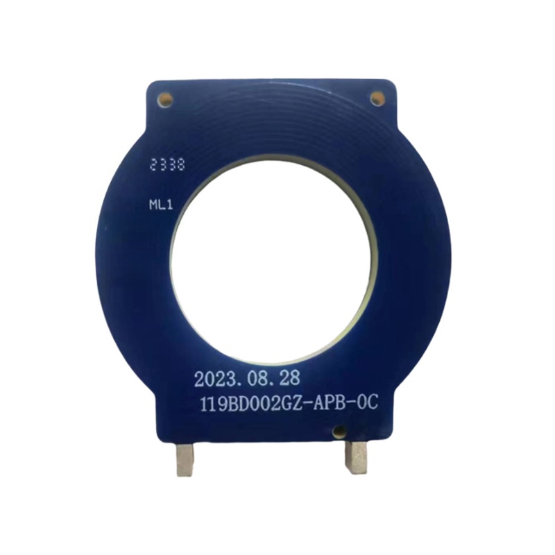
20-layer New Energy High Voltage PCB Manufacturing for EV

SKU:
0.0 (0)
0 Sold
$3.88 $0.00
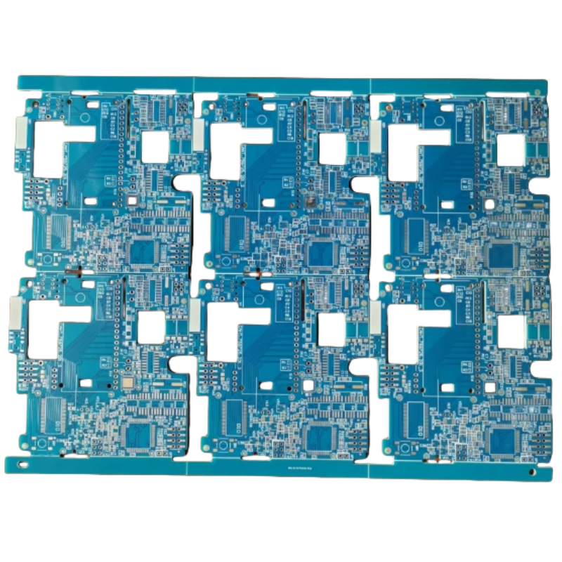
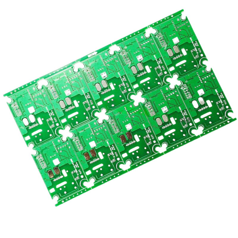
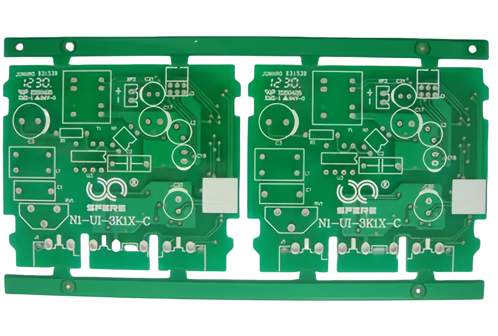
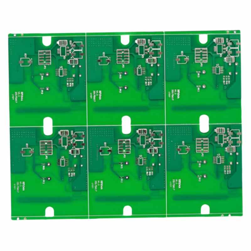
20-layer Inductor Coil PCBs for EVs are built with TU865 material. With 3oz copper, double-pressed process, and POFV tech, they ensure high voltage stability. Lead-free spray tin finish for reliability.
Product Name Inductor Coil PCB
Number of Layers 20 L
Board Thickness 4.0mm
Dimensions 55*62mm
Material TU865
Thickness Ratio 8:1
Minimum Aperture 0.5mm
Minimum Trace Width/Spacing 180/180μm
Product Features 3oz copper; double-pressed; POFV (Plugged Over Via Full)
Surface Treatment Type Lead-free spray tin (HASL - Hot Air Solder Leveling, lead-free)
Received successfully
Coupon Code
CONTINUE SHOPPING
    Please select the information you want X
  • Type:
    SMT PCB assembly: 20 million points/day
    PCB manufacturing: 80,000 m²/month
Quantity:
  • New Energy High Voltage PCB Manufacturing for EV
  • New Energy High Voltage PCB Manufacturing for EV
1/1
  • New Energy High Voltage PCB Manufacturing for EV
  • Description

In the rapidly advancing field of new energy electric vehicles (EVs), the demand for high-performance and reliable printed circuit boards (PCBs) for inductor coils is soaring. Our 20-layer Inductor Coil PCBs are specifically designed to meet the rigorous requirements of high - voltage applications in EVs.

Constructed using TU865 material, these PCBs offer excellent electrical insulation and thermal stability, which are crucial for handling the high voltages and currents encountered in EV power systems. The board thickness of 4.0mm and a thickness ratio of 8:1 ensure sufficient mechanical strength to withstand vibrations and shocks during vehicle operation.

One of the standout features of our PCBs is the use of 3oz copper. This thick copper layer provides low resistance, enabling efficient power transmission and reducing energy losses. The double - pressed manufacturing process further enhances the copper layer's adhesion to the substrate, ensuring long - term reliability under high - stress conditions.

The POFV (Plugged Over Via Full) technology is another key advantage. By filling the vias, it prevents the ingress of moisture and contaminants, reducing the risk of electrical shorts and improving the overall reliability of the PCB. Additionally, the minimum aperture of 0.5mm and minimum trace width/spacing of 180/180μm allow for precise circuit layouts and high - density component placement.

The lead - free spray tin (HASL - Hot Air Solder Leveling, lead - free) surface treatment provides excellent solderability while being environmentally friendly, ensuring reliable component attachment during assembly.

For high - quality high - voltage PCBs for EV inductor coils, contact us at yuan@shwaypcb.com.

CUSTOMER REVIEWS

0.0 0 Reviews
Write a review
Frequently Bought Together
more
Frequently Bought Together