We use cookles to Improve your online experience. By continuing browsing this website, we assume you agree our use of cookies.
$0.00 $0.00
Close
$0.00 $0.00
Home > All Products > Multilayer PCB > 12-layer Manufacturing of multi-layer PCB for server switches
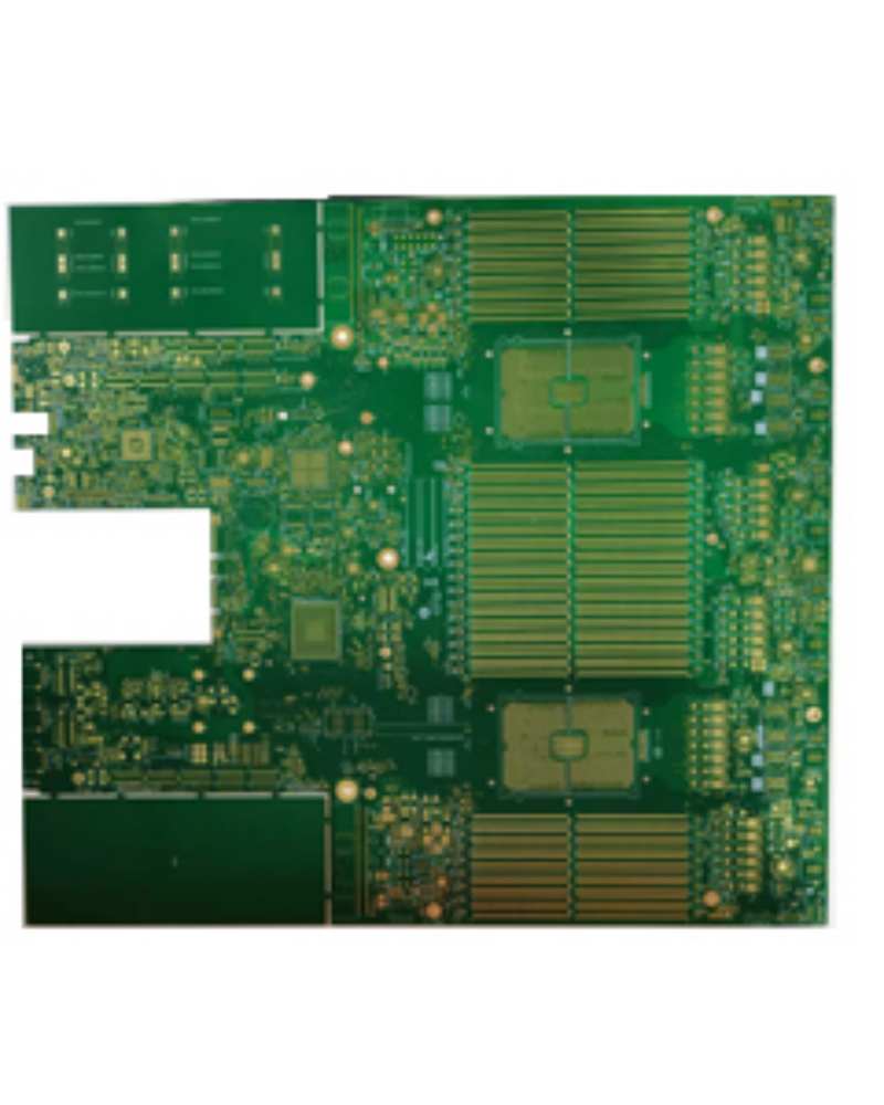
12-layer Manufacturing of multi-layer PCB for server switches

SKU:
0.0 (0)
0 Sold
$3.58 $0.00
We specialize in manufacturing 12-layer server PCBs with precise dimensions of 427.98*479.36mm and a thickness of 1.93mm. Utilizing IT-968G high-speed material, with an aspect ratio of 7.32:1, these PCBs support features like POFV and Skip-via, and feature an ENIG surface finish to meet the stringent requirements of server switches.
Product Name Server PCB
Number of Layers 12 L
Board Thickness 1.93mm
Dimensions 427.98*479.36mm
Material IT-968G
Thickness Ratio 7.32:1
Minimum Aperture 0.25mm
Minimum Trace Width/Spacing 89/100μm
Product Features POFV, High-Speed Material, Skip-via
Surface Treatment Type Immersion Gold (ENIG)
Received successfully
Coupon Code
CONTINUE SHOPPING
    Please select the information you want X
  • Type:
    SMT PCB assembly: 20 million points/day
    PCB manufacturing: 80,000 m²/month
Quantity:
  • Manufacturing of multi-layer PCB for server switches
  • Manufacturing of multi-layer PCB for server switches
1/1
  • Manufacturing of multi-layer PCB for server switches
  • Description

In the field of server switches, a high-quality PCB is of paramount importance. We are dedicated to the manufacturing of 12-layer server PCBs, with precise dimensions of 427.98*479.36mm and a board thickness of 1.93mm. The aspect ratio of 7.32:1 ensures stable operation even under complex circuit layouts.

We use IT-968G high-speed material, which offers excellent electrical performance and signal transmission capabilities. This effectively reduces signal loss and enhances the data processing speed and stability of servers. The PCBs incorporate POFV (Via-in-Pad Plated Over Fill) technology, which strengthens the connection between pads and vias, and Skip-via design, which optimizes routing space and improves circuit integration.

In terms of manufacturing processes, our PCBs feature a minimum via diameter of 0.25mm and a minimum trace width/spacing of 89/100μm, meeting the demands of high-density routing. The surface is finished with Electroless Nickel Immersion Gold (ENIG), enhancing soldering reliability and extending the service life of the PCBs.

We are equipped with advanced production facilities and a stringent quality control system to ensure that every PCB meets high standards. If you have related requirements, please feel free to contact us via email at yuan@shwaypcb.com. We will provide you with professional solutions.

CUSTOMER REVIEWS

0.0 0 Reviews
Write a review
Frequently Bought Together
more
Frequently Bought Together