✅ 1. Cost Advantage and Delivery Efficiency
Price Revolution:
▪ Bulk price: $0.08/cm² (for orders of 100m²)
📉 Cost reduction of 60% compared to 2020 (thanks to the substitution of imported LCP materials with domestic ones and a 25% tariff exemption)
Ultra-Fast Delivery:
⏱️ 48-hour completion of 10-layer board prototyping (compared to an average of 7 days in the US)
🚚 Global Logistics: 3-day air delivery to Europe and the US (via FedEx cross-border express)
⚙️ 2. Core Process Breakthroughs
| Parameter |
Traditional Solution |
Our Solution |
| Minimum line width/spacing |
75/75μm |
40/40μm |
| Interlayer alignment accuracy |
±50μm |
±15μm |
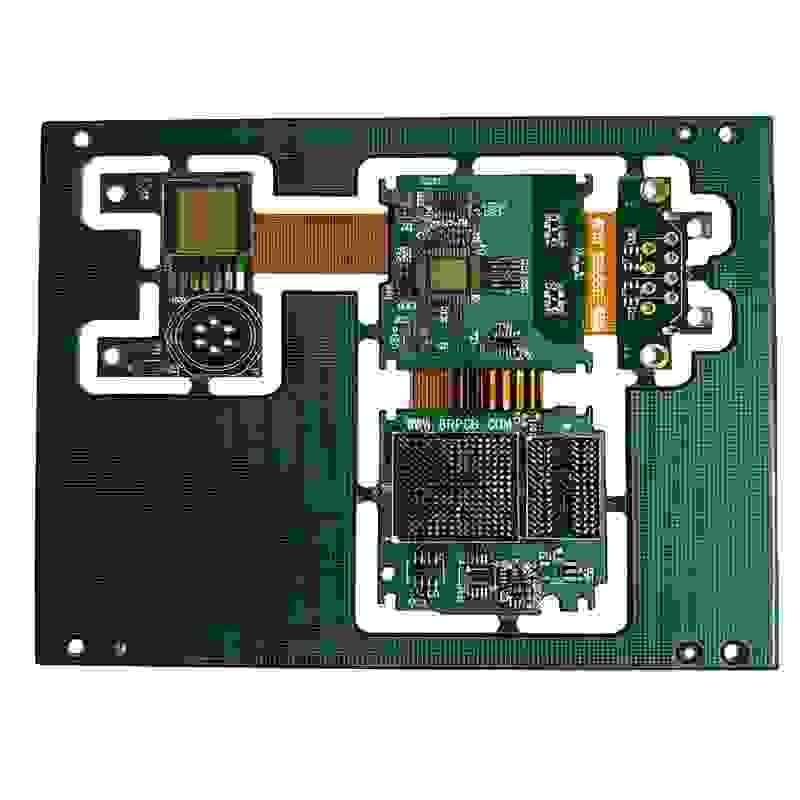
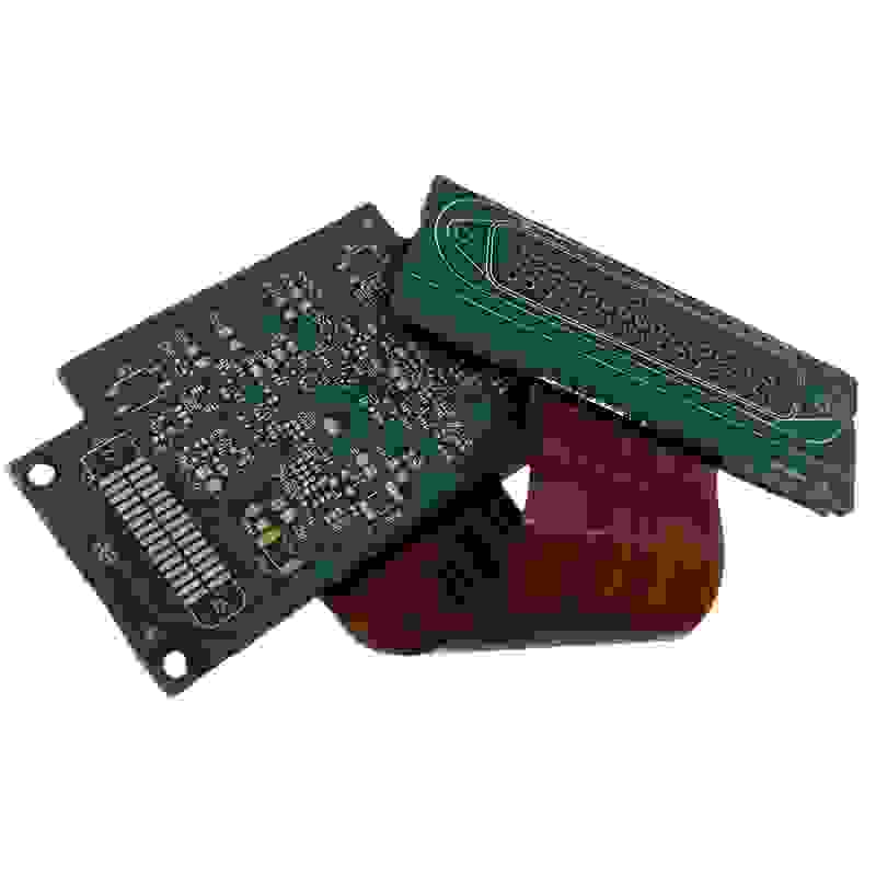
| Rigid-flex transition reliability |
50,000 bending cycles |
200,000 bending cycles |
| Impedance control |
±10% |
±5% |
Technological Innovations:
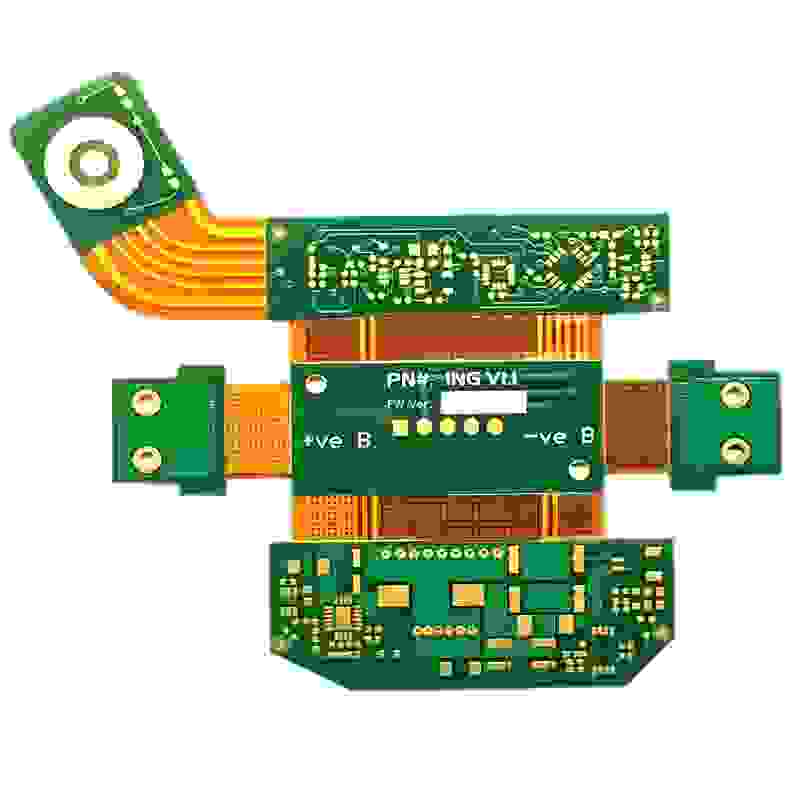
🔧 Composite drilling technology: CO₂ laser + mechanical drilling (30% cost reduction, hole diameter ≤100μm)
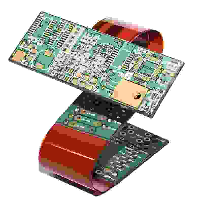
🛡️ Nano-silica gel filling in the rigid-flex zone, with bending stress resistance >150MPa (verified through real-world testing with Huawei's TWS earbuds)
🌐 3. Industry Application Scenarios
Consumer Electronics (accounting for 65% of orders):
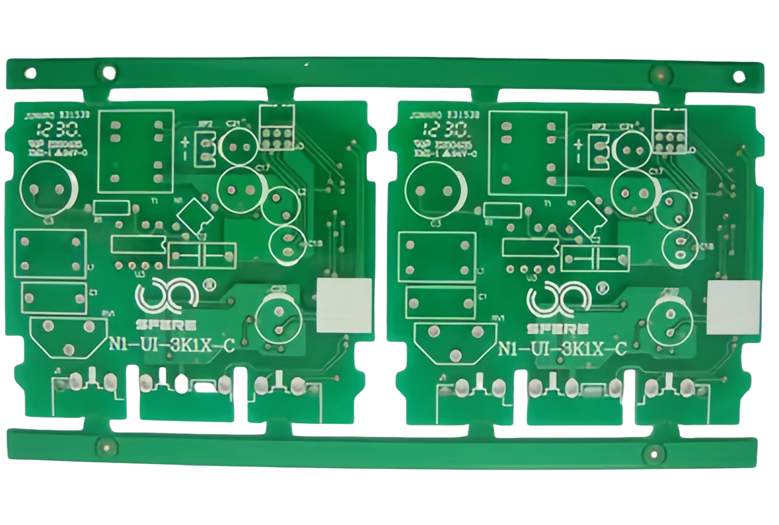
🎧 TWS earbud charging case: 6-layer rigid-flex board with a thickness of 0.25mm and a bending radius that meets a 99.5% reliability standard
Environmental Certifications:
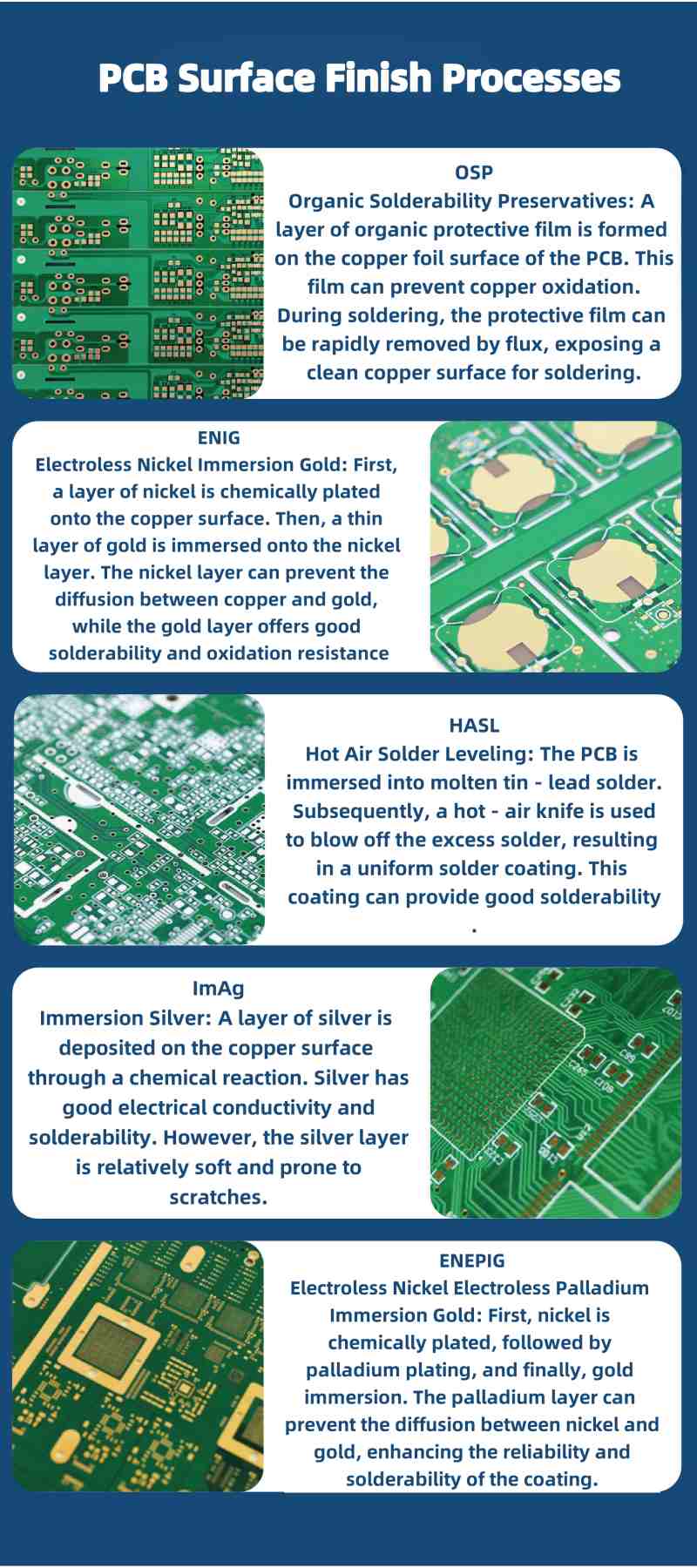
♻️ RoHS 3.0 + cyanide-free immersion gold process (with a gold thickness of 0.05-0.1μm)
🌿 Wastewater reuse rate >95% (exceeding China's GB 8978-2025 standard)
💡 5. Commercial Empowerment Strategies
Free Value-Added Services:
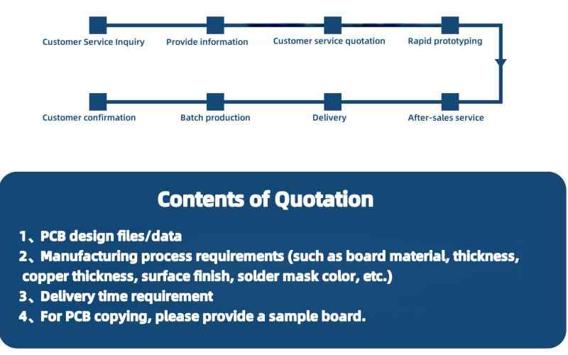
🔧 Online cost calculator: Real-time quotation (covering materials, number of layers, and processes)
📄 Huawei DFM specification library: Open access to 127 design guidelines (to avoid rigid zone cracking)
Scalability Advantages:
🏭 Industrial cluster in the Greater Bay Area: 18% reduction in material procurement costs (within a 100km supply chain radius)
🤖 Automated factory: Per capita output value of $280K/year (3 times the level in Europe and the US)
Why choose us?
I. Superior Tech, Quality Assured
We lead in PCB manufacturing with advanced processes like high-precision drilling, fine-line fabrication (min. 50μm line width/spacing), and multi-layer lamination, meeting high-end routing density needs for stable signal transmission. A strict quality system ensures over 99.5% yield via flying probe and AOI tests. Our expert R&D team offers tailored solutions, from material selection to complex circuit design.
II. Diverse Products, Versatile Solutions
We provide FR-4, high-frequency, metal-core, and flexible boards, each with unique properties for various applications. Mass-produce 2 - 30 layer PCBs for efficient signal and power management. Customize board size, hole diameter, surface finish, and functions to fit specific scenarios.
III. Timely Delivery, Project Assurance
Optimized production and advanced management shorten cycles. We control delivery for double-sided PCBs within [X] days and arrange multi-layer PCBs flexibly. With large capacity and emergency response, we avoid delays. Real-time tracking keeps clients informed.
IV. Competitive Pricing, High Value
Cost-saving measures enable competitive pricing without compromising quality. Transparent quotes detail all costs. Our PCBs excel in price, quality, and delivery, enhancing clients' product competitiveness.
V. Thoughtful Service, High Satisfaction
Our sales team offers pre-sales expertise. Technical support spans design to production. We handle after-sales issues promptly
and conduct follow-ups for continuous improvement.