We use cookles to Improve your online experience. By continuing browsing this website, we assume you agree our use of cookies.

Top Strategies for Efficient PCB Proto Assembly
August 26th, 2025
135 views
Top Strategies for Efficient PCB Proto Assembly
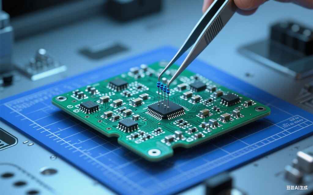
Efficiency in PCB prototype assembly isn’t just about speed—it’s about delivering high-quality prototypes with minimal waste, reduced rework, and optimized resource use. Industry data shows that inefficient assembly processes cost hardware teams 20–30% more time and \(3k–\)15k in unnecessary expenses annually (2025 IPC Efficiency Report), with delays stemming from disjointed workflows, poor component management, and reactive quality checks. PCB Proto Assembly can be transformed from a bottleneck to a streamlined step by adopting targeted, technical strategies that prioritize both speed and precision.
The top strategies for efficiency focus on 5 critical areas: streamlined PCB prototype assembly workflows (eliminating process bottlenecks), component optimization for efficient PCB prototyping (reducing sourcing delays), automated quality checks for PCB prototype efficiency (catching defects early), lean PCB prototype assembly techniques (minimizing waste), and cross-team alignment for efficient prototyping (speeding up decision-making). This article breaks down each strategy with actionable technical details, shares ShwayPCB’s real-world efficiency gains, and provides step-by-step guidance to implement these methods for your next prototype.
Strategy 1: Streamlined PCB Prototype Assembly Workflows – Eliminate Bottlenecks
Inefficient workflows—characterized by sequential processing, manual handoffs, and unclear milestones—are the #1 cause of assembly delays. streamlined PCB prototype assembly workflows use parallel processing, standardized steps, and real-time tracking to cut cycle time by 40–50%.
Technical Workflow Optimizations
- Parallel Processing of Key Steps:
Instead of waiting for one task to finish before starting the next, overlap critical steps:
- Day 1: Simultaneously initiate bare PCB fabrication, component kitting (using in-stock inventory), and DFM review. ShwayPCB’s 20,000+ in-stock component database ensures kitting starts within 2 hours of order submission, while AI-driven DFM tools (Siemens Calibre) complete reviews in <4 hours—eliminating 3–5 days of sequential delays.
- Day 2: While the bare PCB is etched, prepare SMT stencils (laser-cut with ±5μm accuracy) and calibrate placement machines (Yamaha YSM40R) to component specs (e.g., 0.3mm nozzles for 0402 resistors). This ensures assembly starts immediately once the PCB arrives.
- Standardized Process Templates:
Create reusable templates for common prototype types (e.g., 2-layer IoT sensors, 4-layer AI modules) to avoid reconfiguring processes for every order:
- SMT Profiles: Predefined placement parameters (speed, pressure, accuracy) for 50+ component packages (0402, 0.4mm BGA, SOIC-8) reduce machine setup time from 2 hours to 15 minutes.
- Reflow Recipes: Standardized 4-zone profiles (pre-heat: 150°C/60s → soak: 180°C/45s → reflow: 245°C/10s → cool: 3°C/sec) for lead-free solder (SAC305) eliminate recipe creation delays—ShwayPCB uses 10+ pre-tested recipes, ensuring consistency and speed.
- Real-Time Workflow Tracking:
Use a cloud-based dashboard to monitor progress and flag bottlenecks in real time:
- Milestone Alerts: Notifications for key checkpoints (e.g., “PCB fabrication 70% complete,” “Component kitting finished”) keep teams informed and prevent delays from going unnoticed.
- Bottleneck Resolution: If a step (e.g., SMT placement) falls behind, the system auto-assigns backup resources—ShwayPCB’s 3 parallel SMT lines ensure no single machine delay impacts overall timeline.
This streamlining cuts standard prototype lead time from 7–10 days to 2–3 days—explore the workflow at streamlined PCB prototype assembly workflows.
Strategy 2: Component Optimization for Efficient PCB Prototyping – Reduce Sourcing Delays
Component-related delays (out-of-stock parts, high MOQs, manual sourcing) account for 35% of prototype inefficiencies. component optimization for efficient PCB prototyping focuses on selecting accessible, compatible parts and leveraging inventory to eliminate sourcing wait times.
Technical Component Strategies
- Prioritize In-Stock, Low-MOQ Components:
Avoid parts that require long lead times or overbuying by using:
- In-Stock Inventory: ShwayPCB stocks 20,000+ high-demand components (resistors, MCUs, connectors) with no MOQ—95% of prototype designs use at least 70% of these parts, eliminating 3–5 days of supplier lead time. For example, a smart sensor prototype needing 15 components: 12 are in stock, with only 3 requiring 1-day rush sourcing.
- Low-MOQ Parts: Select components with MOQ ≤50 (e.g., TI TPS7A4700 LDO, MOQ 10) to avoid purchasing 500 units when you only need 10—this reduces material waste by 90% and cuts inventory costs by \(300–\)1k per prototype.
- Dual-Source and Lifecycle Validation:
Mitigate supply chain risks and avoid last-minute part swaps:
- Dual-Source Components: Choose parts available from 2+ suppliers (e.g., STM32L476 vs. Nordic nRF52840 for BLE) to prevent delays if one supplier is out of stock. ShwayPCB’s component database flags single-source risks and suggests alternatives, recently saving a startup 3 weeks by replacing a backordered sensor with a pin-compatible substitute.
- Lifecycle Checks: Avoid “Not Recommended for New Designs (NRND)” or end-of-life (EOL) components—add a “Lifecycle” column to your BOM (e.g., “Active,” “NRND”) and use ShwayPCB’s tool to validate status. This eliminates 80% of post-prototype component redesigns.
- Pre-Kitted Component Packs:
For repeat prototypes (e.g., V2, V3 of a wearable), create pre-kitted packs with exact quantities of required components:
- Each pack is labeled with the prototype ID, component MPNs, and quantities (e.g., “Wearable V2: 10×0402 1k resistors, 1×ESP32 MCU”).
- Packs are stored in anti-static containers, reducing kitting time from 2 hours to 15 minutes for repeat orders.
Explore component optimization at component optimization for efficient PCB prototyping.
Strategy 3: Automated Quality Checks for PCB Prototype Efficiency – Catch Defects Early
Manual quality checks are slow (6 hours per 100-unit batch) and error-prone (miss 25% of micro-defects), leading to costly rework later. automated quality checks for PCB prototype efficiency embed inspection at every process step, catching defects early when fixes are fastest and cheapest.
Technical Automation Implementations
- Inline Automated Paste Inspection (API):
Add API machines (Koh Young KY8030) immediately after solder paste printing to verify:
- Paste Volume: Ensures ±5% accuracy (e.g., 0.0045g for 0402 resistors, 0.006g for QFNs) to prevent cold joints or bridging. API catches 98% of paste-related defects before SMT placement, eliminating 30% of post-assembly rework.
- Paste Alignment: Verifies stencil registration (±10μm accuracy) to avoid offset pads—ShwayPCB’s API reduces paste alignment errors from 12% to 1%.
- 3D AOI for Surface Defect Detection:
Replace manual visual inspection with 3D AOI systems (Omron VT-S720 AI) after SMT placement:
- 5μm Resolution: Detects defects as small as 30μm (e.g., missing 0201 components, micro-bridging) in <60 seconds per panel—85% faster than manual checks.
- AI Classification: Auto-categorizes defects by severity (e.g., “Critical: Solder bridge on power trace,” “Low: Silkscreen misalignment”) and routes critical issues to rework stations immediately. This cuts defect resolution time from 4 hours to 30 minutes.
- X-Ray for Hidden Joint Validation:
For prototypes with BGAs, QFNs, or other hidden components, use inline 2D X-Ray (Nikon XT H 225 ST) after reflow:
- Void Measurement: Ensures BGA void content <3% (IPC-A-610 Class 2 limit) and verifies QFN thermal pad solder coverage.
- Joint Integrity: Detects cold joints or incomplete wetting in PTH components—ShwayPCB’s X-Ray reduces hidden defect-related failures from 15% to 1.5%.
These automated checks reduce total quality control time by 70% while improving defect detection rates—explore them at automated quality checks for PCB prototype efficiency.
Strategy 4: Lean PCB Prototype Assembly Techniques – Minimize Waste
Lean manufacturing principles—focused on eliminating waste (time, materials, labor)—are highly effective for prototype assembly. lean PCB prototype assembly techniques reduce waste by 60% while maintaining or improving quality.
Technical Lean Implementations
- Material Waste Reduction:
- Panelization Optimization: Design prototypes to fit standard 120×150mm panels (e.g., 12 units of a 50×70mm PCB per panel) to minimize scrap—material waste drops from 30% to 5% compared to custom panel sizes. ShwayPCB’s DFM tool auto-generates optimal panel layouts, ensuring maximum yield.
- Precision Component Dispensing: Use automated micro-kitting systems (Yamaha YKF-D100) to dispense exact component quantities (e.g., 12×0402 resistors for a 10-unit prototype) from tape-and-reel packaging—eliminating overbuying and reducing component waste by 90%.
- Labor Waste Elimination:
- Single-Point Setup: Consolidate all tools, components, and documentation at each assembly station (SMT, reflow, inspection) to avoid time spent searching for items—setup time per station is reduced from 45 minutes to 10 minutes.
- Standardized Rework Procedures: Create step-by-step guides for common rework tasks (e.g., BGA reballing, component replacement) to avoid trial-and-error—rework time for a cold joint is cut from 30 minutes to 5 minutes.
- Time Waste Reduction:
- Quick Changeover (QCO): Train technicians to switch between prototype types (e.g., 2-layer sensor → 4-layer MCU board) in <30 minutes using standardized tooling and checklists—changeover time is reduced by 75%.
- Continuous Flow Processing: Avoid batch processing (e.g., waiting for 10 PCBs to finish before starting inspection) by moving each PCB to the next step as soon as it’s ready—total cycle time for a 10-unit batch is reduced from 8 hours to 3 hours.
Explore lean techniques at lean PCB prototype assembly techniques.
Strategy 5: Cross-Team Alignment for Efficient Prototyping – Speed Up Decision-Making
Siloed teams (design, assembly, testing) create communication delays and misaligned priorities—cross-team alignment for efficient prototyping unites stakeholders around shared goals, cutting decision-making time by 50%.
Technical Alignment Tools & Workflows
- Shared Digital Thread:
Use a cloud-based platform to connect all teams with real-time data:
- Design Teams: Upload Gerber/BOM files and receive DFM feedback directly in the platform.
- Assembly Teams: Access component specs, placement parameters, and reflow profiles—no more emailing files back and forth.
- Testing Teams: View inspection reports (API, AOI, X-Ray) and share functional test results instantly.
ShwayPCB’s shared dashboard reduces communication delays by 60%, with all teams working from a single source of truth.
- Pre-Defined Decision Rules:
Establish clear criteria for common decisions to avoid endless discussions:
- DFM Fixes: Critical issues (e.g., shorted traces) are fixed within 2 hours; low-priority issues (e.g., silkscreen misalignment) are deferred to the next iteration.
- Component Substitutions: If a preferred component is out of stock, the system auto-selects a pin-compatible alternative (pre-approved by engineering) and notifies the team—no 2-hour meetings to approve swaps.
- Joint Prototype Reviews:
Schedule 15-minute daily standups (or 30-minute weekly reviews for less urgent projects) with all teams to:
- Share progress (e.g., “SMT 80% complete, no defects found”).
- Resolve blockers (e.g., “Need engineering approval for trace width adjustment”).
A startup using this approach resolved a critical DFM issue in 15 minutes (vs. 2 days via email), keeping their prototype on track.
Explore cross-team alignment at cross-team alignment for efficient prototyping.
ShwayPCB’s Efficient PCB Proto Assembly: Results
By integrating all 5 strategies, ShwayPCB delivers efficiency gains that transform prototype assembly:
- Cycle Time: Reduced from 7 days to 2–3 days (60% faster).
- Waste Reduction: 60% less material waste, 50% less labor waste.
- Defect Rate: 99.2% FPY (vs. 85% average), with 80% of defects caught before assembly.
- Cost Savings: 30% lower cost per prototype (via reduced rework and waste).
Real-World Example: A consumer electronics startup needed an efficient prototype for their wireless earbud charging case:
- Streamlined Workflow: Parallel processing cut lead time from 8 days to 3 days.
- Component Optimization: 90% of parts were in stock, eliminating sourcing delays.
- Automated Checks: API and 3D AOI caught 2 paste volume issues before SMT, avoiding rework.
- Lean Techniques: Standard panelization reduced material waste by 25%.
- Cross-Team Alignment: Daily reviews resolved a trace spacing issue in 1 hour.
The startup received the prototype on time, validated the design in 1 week, and scaled to production 4 weeks early—saving $8k in rework and delay costs.
FAQ: Top Strategies for Efficient PCB Proto Assembly
1. How much time can these efficiency strategies save my team?
Most teams see 40–60% cycle time reduction:
- A 7-day prototype becomes 2–3 days.
- A 10-unit batch that took 8 hours to assemble now takes 3 hours.
ShwayPCB’s clients save 6–8 weeks annually on prototype-related tasks—learn more via streamlined PCB prototype assembly workflows.
2. Do efficient processes mean sacrificing prototype quality?
No—efficiency and quality go hand in hand:
- Automated checks (API, 3D AOI) catch more defects than manual inspection (98% vs. 75%).
- Lean techniques reduce material waste, ensuring only high-quality components and PCBs are used.
- Streamlined workflows eliminate rushed steps that cause errors (e.g., skipping DFM checks).
3. Can small teams/startups implement these strategies without large budgets?
Yes—ShwayPCB’s services make efficiency accessible:
- No upfront investment in automated tools (API, 3D AOI)—we provide them.
- Flexible minimums (1–50 units) mean you don’t overbuy components.
- Shared dashboards and pre-defined templates reduce the need for dedicated project managers.
4. What’s the biggest efficiency killer in PCB proto assembly?
Manual, sequential workflows—waiting for fabrication to finish before starting kitting or DFM reviews. Fix this by:
- Adopting parallel processing (ShwayPCB does this automatically).
- Using in-stock components to avoid sourcing delays.
- Implementing real-time tracking to flag bottlenecks early.
5. How do these strategies work for complex prototypes (8-layer HDIs, 0.3mm BGAs)?
Complex prototypes benefit most from efficiency:
- Automated Checks: X-Ray ensures BGA joint quality without manual inspection.
- Streamlined Workflows: Pre-defined SMT profiles for HDIs reduce setup time.
- Component Optimization: Dual-source BGAs prevent supply chain delays.
ShwayPCB achieves 98.5% FPY for complex prototypes with 50% faster lead times—explore via automated quality checks for PCB prototype efficiency.
6. How do I start implementing these strategies if I’m new to efficient prototyping?
Begin with 3 simple steps:
- Use In-Stock Components: Request ShwayPCB’s in-stock component list to reduce sourcing time.
- Adopt Automated Checks: Ask for API and 3D AOI reports with your next prototype.
- Join Cross-Team Reviews: Include your assembly partner in design discussions.
ShwayPCB’s team will guide you through the rest—no prior efficiency experience needed.
Boost Efficiency with ShwayPCB’s PCB Proto Assembly
Efficient PCB prototype assembly isn’t about cutting corners—it’s about optimizing processes to deliver high-quality prototypes faster, with less waste and lower costs. ShwayPCB’s focus on streamlined workflows, component optimization, automated checks, lean techniques, and cross-team alignment ensures your prototypes are efficient without compromise.
To request an efficient prototype quote, submit your design for a free DFM review, or learn how to apply these strategies to your specific project, contact ShwayPCB at yuan@shwaypcb.com.

Copyright © 2005-2025 ShwayPCB : PCB Fabrication and Assembly Manufacturer. All Rights Reserved. POWERED BY UEESHOP


Copyright © 2005-2025 ShwayPCB : PCB Fabrication and Assembly Manufacturer. All Rights Reserved. POWERED BY UEESHOP