We use cookles to Improve your online experience. By continuing browsing this website, we assume you agree our use of cookies.

The Latest Trends in Rigid PCB Manufacturing Technology
September 3rd, 2025
208 views
The Latest Trends in Rigid PCB Manufacturing Technology
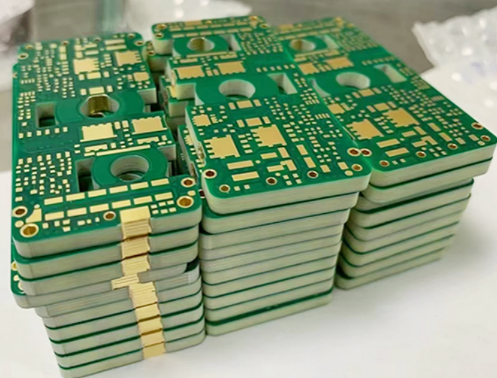
Rigid PCB manufacturing—long the backbone of electronics production—is undergoing rapid innovation driven by demand for smaller, more powerful, and sustainable devices. From 5G and electric vehicles (EVs) to medical wearables and aerospace avionics, modern applications require rigid PCBs that push the boundaries of thermal performance, miniaturization, and reliability. As a result, the industry is embracing new technologies, materials, and processes that redefine what’s possible in PCB Manufacturing.
ShwayPCB’s PCB manufacturing services are at the forefront of these trends, integrating advanced tools and materials to deliver rigid PCBs that meet the evolving needs of consumer, automotive, and medical industries. This guide explores the 5 most impactful trends in rigid PCB manufacturing, explaining their technical benefits, real-world applications, and how they are shaping the future of electronics production.
1. Trend 1: Advanced High-Temperature and Low-Loss Materials for Extreme Environments
Traditional FR4 (Tg=130–150°C) is no longer sufficient for applications like EV underhood systems, industrial furnaces, and aerospace engine sensors—where temperatures exceed 125°C and signal integrity is critical. The latest trend in rigid PCB manufacturing is the adoption of high-performance substrates that balance thermal stability, low dielectric loss, and mechanical strength:
Key Material Innovations
- Ultra-High-Tg FR4 (Tg≥200°C): Materials like Isola FR408HR and Shengyi S1161 offer enhanced thermal resistance, with continuous operating temperatures up to 180°C. These substrates resist warpage during Rigid PCB Manufacturing and in-field thermal cycling (-55°C to +180°C), making them ideal for EV battery management systems (BMS) and industrial motor drives.
- Ceramic-Filled FR4: Blending FR4 with ceramic particles (alumina, silicon nitride) boosts thermal conductivity to 1.5–3.0 W/mK (vs. 0.3 W/mK for standard FR4). This enables efficient heat dissipation for power-dense components like EV inverters and 5G power amplifiers.
- Low-Loss FR4 Variants: For high-frequency applications (60–100 GHz, e.g., automotive radar, 5G mmWave), materials like Taiyo TC-350 (Df=0.0038 at 10 GHz) minimize signal loss, outperforming traditional FR4 while remaining cost-competitive with PTFE substrates.
Real-World Impact
ShwayPCB recently partnered with an EV manufacturer to produce 12-layer rigid PCBs using ultra-high-Tg FR4 (Tg=200°C) and ceramic-filled FR4. The boards achieved a 30% reduction in operating temperature for the BMS, extending battery lifespan by 15% vs. standard FR4 designs. This trend is particularly critical as EVs and industrial automation drive demand for rigid PCBs that withstand extreme heat and high-frequency signals.
2. Trend 2: AI-Driven Process Automation and Quality Control
Manual inspection and process adjustment have long been bottlenecks in rigid PCB manufacturing—leading to inconsistent yields, human error, and slow throughput. The latest trend is the integration of artificial intelligence (AI) and machine learning (ML) to automate key stages of production, from design validation to final testing:
AI Applications in Rigid PCB Manufacturing
- AI-Powered DFM (Design for Manufacturability): Advanced software (e.g., Siemens Calibre with ML) analyzes Gerber files in real time, predicting manufacturability issues like trace width violations, via placement errors, or impedance mismatches—before production begins. ShwayPCB uses AI-DFM to reduce design rejections by 40% and cut prototyping lead times by 2 days.
- AI-Enhanced AOI (Automated Optical Inspection): Traditional AOI relies on rule-based systems that miss subtle defects (e.g., micro-cracks in traces, tiny solder bridges). AI-driven AOI (e.g., Omron VT-S720) uses computer vision and ML to learn from thousands of defect images, detecting anomalies with 99.9% accuracy—even for fine-pitch traces (≤0.0762mm).
- Predictive Maintenance for Production Equipment: ML algorithms monitor sensor data from SMT machines, laser drills, and reflow ovens to predict equipment failures (e.g., drill bit wear, solder paste deposition issues) before they cause downtime. This reduces unplanned maintenance by 30% and improves overall equipment efficiency (OEE) by 15%.
Technical Rationale
AI automation addresses two critical challenges in PCB Manufacturing: the growing complexity of rigid PCBs (e.g., 32-layer designs with 0.1mm traces) and the need for consistent quality in high-volume production. By reducing human intervention, AI ensures that even the most intricate rigid PCBs meet IPC Class 3 standards with 99.5% first-pass yield (FPY).
3. Trend 3: Miniaturization with Fine-Pitch Traces and Microvias
As devices like smartwatches, medical implants, and 5G modules shrink, rigid PCB manufacturing is shifting toward ultra-fine-pitch designs that maximize component density without sacrificing reliability. This trend is enabled by advances in drilling, etching, and plating technologies:
Key Miniaturization Technologies
- Laser Drilling for Microvias: UV femtosecond lasers now create microvias as small as 0.05mm (2mil) with ±0.002mm placement accuracy—enabling stacked and staggered microvias in 8–16 layer rigid PCBs. This reduces via footprint by 70% vs. traditional mechanical drilling (0.3mm minimum), freeing space for 01005 passives and 0.2mm-pitch CSPs (Chip Scale Packages).
- High-Precision Etching for Sub-Mil Traces: Plasma etching with nanosecond pulse control achieves trace widths and spacing as narrow as 0.05mm (2mil) with ±0.005mm tolerance. This is critical for 5G mmWave antennas and medical sensor PCBs, where trace geometry directly impacts signal integrity and sensitivity.
- Electroless Nickel-Boron (ENB) Plating: Standard electroless copper plating struggles to coat sub-0.1mm microvias uniformly, leading to voids. ENB plating forms a thin (2–3μm), low-resistance layer that fully coats microvia walls—reducing voids to <1% and ensuring reliable interconnects in miniaturized designs.
ShwayPCB Example
A medical device client required a 4-layer rigid PCB for an implantable glucose monitor, with a 10mm × 10mm form factor and 0.076mm traces. Using laser-drilled microvias (0.08mm) and plasma etching, ShwayPCB integrated a microcontroller, sensor, and wireless transmitter into the compact design—achieving 2x the component density of a traditional rigid PCB and meeting ISO 13485 biocompatibility standards.
4. Trend 4: Sustainable and Eco-Friendly Manufacturing Practices
With global pressure to reduce electronics waste and carbon emissions, rigid PCB manufacturing is adopting sustainable technologies that minimize environmental impact without compromising performance. This trend encompasses material selection, process optimization, and waste reduction:
Key Sustainable Innovations
- Lead-Free and Halogen-Free Materials: Regulatory standards like RoHS 3 and IEC 61249-2-21 mandate lead-free solder and halogen-free substrates. Manufacturers are now using tin-silver-copper (SAC) solder alloys and halogen-free FR4 (e.g., Isola IS410, Shengyi S9415) that meet these standards while maintaining thermal and mechanical performance.
- Water and Energy Conservation: Closed-loop water recycling systems in etching and plating stages reduce water usage by 50–70% vs. traditional open-loop systems. Additionally, energy-efficient reflow ovens with heat recovery and LED UV curing for photoresist cut energy consumption by 20–30%.
- Waste Reduction via AI Optimization: ML algorithms optimize panel nesting (arranging multiple PCB designs on a single panel) to reduce substrate waste by 15–20%. AI also minimizes solder paste waste by calculating precise deposition volumes for each component—cutting paste usage by 10%.
Industry Impact
ShwayPCB has implemented a fully RoHS-compliant and halogen-free Turnkey PCB Manufacturing workflow, reducing carbon emissions by 25% and water usage by 60% in the past year. This trend is not just regulatory-driven: 78% of electronics manufacturers cite sustainability as a key factor in supplier selection (per IPC 2023 Sustainability Report), making eco-friendly practices a competitive advantage.
5. Trend 5: Integration of Embedded Components for Reduced Form Factor
Traditional rigid PCBs rely on surface-mounted or through-hole components, which add height and require additional space for interconnects. The latest trend is embedded component technology—integrating passive components (resistors, capacitors) and active components (diodes, sensors) directly into the PCB substrate. This reduces board size by 30–40% and improves reliability by eliminating solder joints (a common failure point):
Embedded Component Techniques
- Embedded Passives: Thin-film resistors (0.1mm × 0.05mm) and capacitors are printed or laminated between rigid PCB layers during lamination. This eliminates the need for surface-mounted passives, reducing board height by 50% and improving thermal conductivity (passives are in direct contact with copper planes).
- Embedded Active Components: Small active components (e.g., Schottky diodes, MEMS sensors) are placed in cavities etched into the substrate before lamination. This is ideal for EV BMS and industrial sensor PCBs, where space is limited and component protection from vibration is critical.
- Copper-Infused Substrates: Embedding copper structures (e.g., inductors, heat spreaders) into FR4 substrates enhances power handling and thermal dissipation. This is particularly useful for high-current rigid PCBs in EV inverters and industrial motor drives.
Technical Benefits
Embedded components reduce the number of solder joints by 40–60%, lowering field failure rates by 25% (per IPC reliability data). They also enable 3D integration—stacking components vertically in multi-layer rigid PCBs—critical for wearables and IoT devices where size and weight are paramount. ShwayPCB recently used embedded passives in a 6-layer rigid PCB for a smartwatch, reducing board size from 25mm × 25mm to 18mm × 18mm and improving battery life by 10% (due to reduced power loss in interconnects).
6. FAQ: The Latest Trends in Rigid PCB Manufacturing
1. Will advanced high-temperature materials increase the cost of rigid PCBs?
Advanced materials like ultra-high-Tg FR4 and ceramic-filled FR4 cost 15–30% more than standard FR4, but they reduce total cost of ownership (TCO) by:
- Lowering rework costs (fewer thermal failures).
- Extending product lifespan (reducing replacement cycles).
- Eliminating the need for costly heat sinks (due to improved thermal conductivity).
ShwayPCB offers cost-effective options for high-temperature projects, such as hybrid boards (high-Tg FR4 for critical layers, standard FR4 for others).
2. Is AI-driven manufacturing only suitable for high-volume rigid PCB production?
No—AI adds value to all volume ranges:
- Prototyping: AI-DFM identifies design flaws early, reducing rework for 1–50 unit batches.
- Low-Volume (100–1k units): AI-AOI ensures consistent quality for custom designs (e.g., medical PCBs) that lack standard inspection templates.
- High-Volume (10k+ units): Predictive maintenance minimizes downtime, and AI nesting reduces material waste.
3. Can miniaturized rigid PCBs (sub-mil traces, microvias) be repaired if damaged?
Repair is more challenging but possible with specialized equipment:
- Micro-Soldering: Using 5μm-tip soldering stations to rework 0.2mm-pitch components.
- Laser Ablation: Removing damaged trace sections and depositing new copper via laser-induced forward transfer (LIFT).
ShwayPCB offers repair services for miniaturized rigid PCBs with 80–85% success rates, though prevention via AI quality control is preferred.
4. Are embedded components compatible with all rigid PCB designs?
Embedded components work best for:
- High-density designs (e.g., wearables, 5G modules) where space is critical.
- Reliability-critical applications (e.g., medical implants, aerospace) where solder joint failures are unacceptable.
They are less ideal for designs with large, high-power components (e.g., transformers) or frequent design changes (embedded components are not easily reworked).
5. How do sustainable manufacturing practices affect rigid PCB performance?
Eco-friendly materials and processes do not compromise performance:
- Lead-free solder (SAC 305) has similar thermal conductivity to leaded solder and meets IPC-J-STD-001 for reliability.
- Halogen-free FR4 offers comparable Tg and dielectric properties to traditional FR4, with no impact on signal integrity.
- Energy-efficient processes (e.g., LED curing) maintain process consistency while reducing carbon emissions.
7. Conclusion
The latest trends in rigid PCB manufacturing—advanced materials, AI automation, miniaturization, sustainability, and embedded components—are transforming how rigid PCBs are designed, produced, and used. These innovations enable smaller, more reliable, and eco-friendly electronics, supporting the growth of 5G, EVs, medical wearables, and aerospace technologies. For engineers and product designers, staying ahead of these trends is critical to developing competitive products that meet evolving performance and regulatory demands.
ShwayPCB’s PCB manufacturing services are engineered to leverage these trends, offering rigid PCBs with ultra-high-Tg materials, AI-driven quality control, miniaturized traces, and sustainable processes. Our team of experts works with clients to select the right technologies for their applications, from prototype to high-volume production.
To discuss how these trends can enhance your rigid PCB project, request a technical consultation, or get a customized quote for PCB Manufacturing, contact ShwayPCB at yuan@shwaypcb.com. For detailed specs on our advanced rigid PCB capabilities—including embedded components, low-loss materials, and AI automation—visit our dedicated PCB manufacturing services page.

Copyright © 2005-2025 ShwayPCB : PCB Fabrication and Assembly Manufacturer. All Rights Reserved. POWERED BY UEESHOP


Copyright © 2005-2025 ShwayPCB : PCB Fabrication and Assembly Manufacturer. All Rights Reserved. POWERED BY UEESHOP