We use cookles to Improve your online experience. By continuing browsing this website, we assume you agree our use of cookies.

Real-Life Applications of Multi-Layer PCB Fabrication in Aerospace Systems
September 3rd, 2025
179 views
Real-Life Applications of Multi-Layer PCB Fabrication in Aerospace Systems
Aerospace systems—from commercial airliners to satellites and fighter jets—operate in the most demanding environments on Earth (and beyond): extreme temperatures (-65°C to +150°C), intense vibration (20–2,000Hz), radiation exposure (up to 100 krad), and strict weight constraints (every gram impacts fuel efficiency). Traditional single-layer PCBs cannot meet these requirements—they lack the density to support compact avionics, the signal integrity for high-frequency radar, and the durability to withstand aerospace stressors.
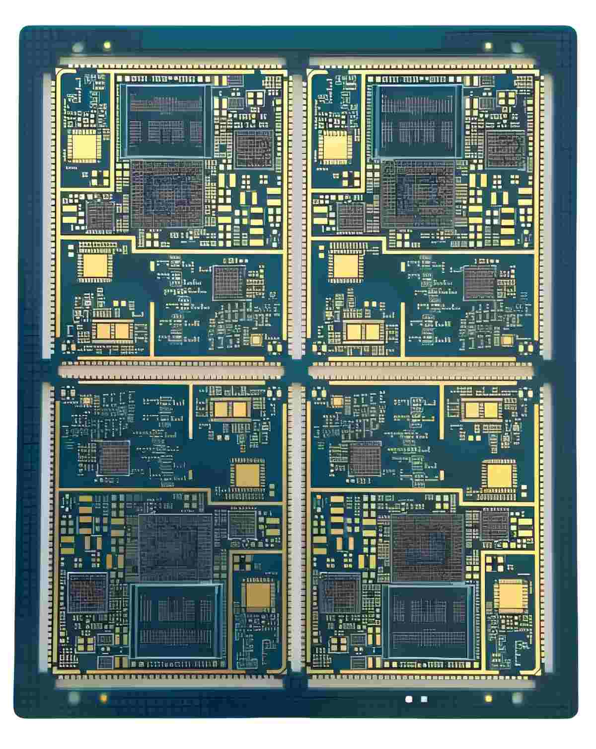
Multilayer PCB Manufacturing has emerged as a cornerstone of modern aerospace engineering, enabling the miniaturization, reliability, and performance that define next-gen aerospace systems. This article explores 5 real-life applications of multi-layer PCBs in aerospace, highlighting how specialized fabrication techniques (e.g., sequential lamination, radiation-hardened materials) address industry-specific challenges. ShwayPCB’s multilayer PCB manufacturing services support these applications, delivering AS9100-certified boards with 10+ year operational lifespans in space and aviation environments.
1. Avionics Control Systems (Commercial & Military Aircraft)
Avionics systems—including flight control, navigation, and engine monitoring—require PCBs that integrate hundreds of components into tight spaces while ensuring 99.999% uptime (a single failure can lead to catastrophic consequences).
Real-Life Application: Boeing 787 Dreamliner Flight Control Unit
- Challenge: The 787’s fly-by-wire system requires a compact control unit that integrates 4 microprocessors, 8 analog-to-digital converters (ADCs), and 16 sensor inputs—all within a 200mm × 250mm footprint. Traditional 4-layer PCBs could not fit these components without sacrificing signal isolation.
- Multi-Layer PCB Solution: A 16-layer multi-layer PCB using sequential lamination:
- Stack-Up: 4 signal layers (flight control signals, sensor data), 2 power layers (28V aircraft power), and 10 ground planes (for EMI isolation).
- Materials: High-Tg FR4 (Tg≥200°C) to withstand engine bay temperatures, and rolled copper (99.99% purity) for low-resistance power traces.
- Performance: Achieves <0.1μs latency for flight control signals, crosstalk < -50dB at 1GHz, and withstands 10G vibration (MIL-STD-883H) without trace cracking.
Key Role of Multi-Layer PCBs
- Density: 16-layer PCBs fit 3x more components than 8-layer designs, reducing the control unit’s size by 40% vs. traditional PCBs.
- Reliability: ShwayPCB’s High-Precision Multilayer PCB fabrication ensures ±0.005mm layer alignment, eliminating short circuits from misaligned traces—critical for flight safety.
2. Aerospace Radar and Communication Systems
Radar (e.g., weather radar, air-to-air surveillance) and satellite communication systems rely on high-frequency signals (77GHz for radar, 1–40GHz for satellite links) that require PCBs with ultra-low signal loss and EMI shielding.
Real-Life Application: Lockheed Martin F-35 Lightning II AESA Radar
- Challenge: The F-35’s Active Electronically Scanned Array (AESA) radar uses 1,600+ transmit/receive (T/R) modules, each requiring 50Ω controlled impedance traces and minimal insertion loss (<0.3dB/cm at 77GHz). Single-layer PCBs suffer from >1dB/cm loss at these frequencies.
- Multi-Layer PCB Solution: A 24-layer RF Multilayer PCB Manufacturing design:
- Materials: Rogers 4350B substrate (Df=0.0037 at 10GHz) for low dielectric loss, and gold-plated copper traces (0.1μm Au) for corrosion resistance.
- Design Features: Dedicated ground planes between every RF layer, blind vias (0.08mm) for T/R module connections, and copper pour shielding to reduce EMI.
- Performance: Insertion loss of 0.25dB/cm at 77GHz, enabling the radar to detect targets 150+ km away—20% farther than legacy radar systems.
Key Role of Multi-Layer PCBs
- Signal Integrity: Separate RF layers and low-loss materials preserve radar signal quality, while ground planes eliminate cross-talk between T/R modules.
- Thermal Management: 4oz copper power planes dissipate 200W of heat from T/R modules, keeping temperatures <85°C during extended missions.
3. Satellite Payload Electronics (Low-Earth Orbit & Geostationary Satellites)
Satellite payloads (e.g., imaging sensors, communication transponders) operate in vacuum, extreme temperature cycles (-65°C to +125°C), and high radiation—requiring PCBs that resist radiation-induced degradation and thermal stress.
Real-Life Application: SpaceX Starlink Satellite Communication Transponder
- Challenge: Starlink satellites require a compact transponder to handle 4G/5G signals, withstanding 100 krad of radiation and 500+ thermal cycles (day/night in orbit). Traditional PCBs fail within 6 months due to radiation-induced copper corrosion.
- Multi-Layer PCB Solution: An 18-layer radiation-hardened multi-layer PCB:
- Materials: Radiation-hardened FR4 (RHFR4) substrate (resists 300 krad), and electroless nickel-phosphorus (Ni-P) plated vias (10μm Ni-P) to prevent radiation-induced opens.
- Design Features: Stacked vias (0.1mm) for payload connections, polyimide conformal coating (50μm) for vacuum compatibility, and symmetric stack-up to avoid warpage.
- Performance: Operates reliably for 5+ years in orbit, with <5% performance degradation after 100 krad exposure.
Key Role of Multi-Layer PCBs
- Radiation Hardening: Specialized materials and plating prevent radiation-induced defects (e.g., via opens, trace corrosion) that disable satellite electronics.
- Miniaturization: 18-layer PCBs reduce the transponder’s volume by 50% vs. 8-layer designs, enabling Starlink to fit 40+ transponders per satellite.
4. Unmanned Aerial Vehicle (UAV) Navigation and Surveillance Systems
UAVs (e.g., military drones, agricultural UAVs) require lightweight, compact electronics that integrate GPS, cameras, and telemetry—often in payloads weighing <500g.
Real-Life Application: General Atomics MQ-9 Reaper UAV Navigation System
- Challenge: The MQ-9’s navigation system combines GPS (1.575GHz), inertial measurement unit (IMU), and telemetry (2.4GHz), requiring 3 separate signal types to coexist without interference. Single-layer PCBs suffer from >-30dB crosstalk between GPS and telemetry signals.
- Multi-Layer PCB Solution: A 12-layer multi-layer PCB:
- Stack-Up: GPS (Layer 1–2), IMU (Layer 3–4), telemetry (Layer 5–6), with ground planes (Layer 7–12) separating each signal type.
- Materials: Lightweight FR4 (density 1.8 g/cm³) to reduce payload weight, and immersion silver finish (0.15μm Ag) for cost-effectiveness.
- Performance: Crosstalk < -45dB between GPS and telemetry, enabling <1m GPS positioning accuracy and 50km telemetry range—critical for precision strikes and surveillance.
Key Role of Multi-Layer PCBs
- Signal Isolation: Ground planes between signal layers eliminate interference, while compact design reduces the navigation system’s weight to 120g—30% lighter than legacy systems.
- Durability: Sequential lamination creates a rigid structure that withstands 15G vibration during takeoff/landing.
5. Aerospace Power Distribution Units (PDUs)
PDUs manage power flow in aircraft/satellites (e.g., 28V DC for avionics, 400Hz AC for engines), requiring PCBs that handle high currents (50–100A) and protect against short circuits.
Real-Life Application: Airbus A350 PDU for Engine Power Management
- Challenge: The A350’s PDU distributes 100A to engine control units, requiring PCBs that avoid overheating and short circuits. Traditional PCBs use bulky bus bars, increasing weight and size.
- Multi-Layer PCB Solution: A 10-layer Heavy Copper Multilayer PCB design:
- Materials: 12oz copper power planes (current capacity 120A) and flame-retardant FR4 (UL94 V-0) for fire safety.
- Design Features: Thermal vias (0.2mm) in a 0.5mm grid under power components, overcurrent protection traces (narrowed 0.05mm sections), and solder mask dams to prevent short circuits.
- Performance: Handles 100A continuous current with <5°C temperature rise, and triggers overcurrent protection in <1ms—preventing engine damage from power surges.
Key Role of Multi-Layer PCBs
- High-Current Handling: Heavy copper planes replace bulky bus bars, reducing PDU weight by 25% and size by 30%.
- Safety: Overcurrent protection traces and flame-retardant materials meet aerospace fire standards (FAA Part 25.853).
6. FAQ: Multi-Layer PCBs in Aerospace Systems
1. What aerospace standards do multi-layer PCBs need to comply with?
Critical standards include:
- AS9100: Quality management for aerospace manufacturing (ShwayPCB is AS9100-certified).
- MIL-STD-883H: Environmental testing (thermal cycling, vibration, radiation).
- IPC-A-600 Class 3: Highest quality class for PCBs (no defects, 100% inspection).
- FAA Part 25: Fire safety (flame-retardant materials, smoke toxicity).
2. How do multi-layer PCBs resist radiation in satellites?
Radiation resistance is achieved via:
- Materials: Radiation-hardened substrates (RHFR4) and plating (Ni-P, Au) that prevent copper corrosion and via opens.
- Design: Redundant traces and vias (e.g., 2 vias per connection) to bypass radiation-damaged paths.
- Testing: Irradiation testing (Co-60 gamma rays) to verify performance up to 300 krad.
3. What is the typical lifespan of multi-layer PCBs in aerospace applications?
- Commercial Aircraft: 15–20 years (e.g., Boeing 787 avionics PCBs).
- Satellites: 5–15 years (Starlink PCBs: 5+ years; geostationary satellites: 15+ years).
- UAVs: 5–10 years (MQ-9 PCBs: 8+ years).
ShwayPCB’s aerospace PCBs undergo accelerated life testing (1,000 thermal cycles) to validate lifespan.
4. Can multi-layer PCBs reduce aerospace system weight?
Yes—multi-layer PCBs enable:
- Component Integration: 16-layer PCBs replace 2–3 single-layer PCBs, reducing weight by 40–50%.
- Eliminating Interconnects: Blind/buried vias replace heavy connectors between boards, saving 10–15% of system weight.
For example, the F-35’s AESA radar uses 24-layer PCBs to reduce weight by 25kg vs. legacy radar systems.
5. What is the lead time for aerospace multi-layer PCB fabrication?
Lead times depend on complexity:
- 12–18 layers: 8–10 weeks (prototyping); 12–14 weeks (mass production).
- 20–32 layers: 10–12 weeks (prototyping); 14–16 weeks (mass production).
ShwayPCB maintains stock of aerospace-grade materials (Rogers 4350B, RHFR4) to reduce lead times by 2–3 weeks.
7. Conclusion
Multi-Layer PCB Fabrication is not just a manufacturing choice for aerospace systems—it is a enabler of innovation, enabling smaller, lighter, and more reliable electronics that withstand the industry’s harshest conditions. From avionics control units that ensure flight safety to satellite PCBs that operate for years in orbit, multi-layer PCBs solve aerospace’s unique challenges by balancing density, signal integrity, and durability.
ShwayPCB’s multilayer PCB manufacturing services are tailored to aerospace needs, with AS9100 certification, radiation-hardened material expertise, and 100% compliance with MIL-STD-883H. Our team of aerospace engineers works with you to optimize every aspect of the PCB—from material selection to stack-up design—ensuring your system meets the strictest performance and reliability standards.
To discuss your aerospace multi-layer PCB project, request radiation testing data, or get a customized quote for Multilayer PCB Manufacturing, contact ShwayPCB at yuan@shwaypcb.com. For detailed case studies (e.g., F-35 radar PCBs, Starlink satellite PCBs) and aerospace material specs, visit our dedicated multilayer PCB manufacturing services page.

Copyright © 2005-2025 ShwayPCB : PCB Fabrication and Assembly Manufacturer. All Rights Reserved. POWERED BY UEESHOP


Copyright © 2005-2025 ShwayPCB : PCB Fabrication and Assembly Manufacturer. All Rights Reserved. POWERED BY UEESHOP