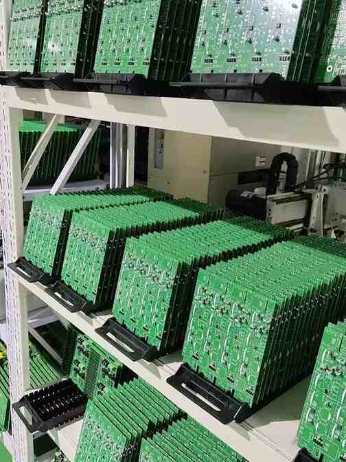
In the electronics manufacturing landscape, printed circuit boards (PCBs) act as the core infrastructure for devices across automotive, medical, IoT, and telecommunications sectors. The dependability of these devices is directly tied to the quality of PCB fabrication and assembly—even tiny flaws like defective solder joints or trace etching errors can trigger system breakdowns, safety risks, or expensive rework. To lower risks and guarantee consistent performance, manufacturers must follow strict quality control (QC) procedures throughout the production cycle. Below, we outline the top practices for QC in PCB fabrication and assembly, incorporating key industry terms that link to expert solutions.
Quality control starts prior to production, specifically during the PCB design phase. DFM/DFA Analysis (Design for Manufacturability/Design for Assembly) is a proactive QC measure that aligns design specifications with practical manufacturing capabilities. By working with engineers to assess layouts, component placement, pad dimensions, and trace widths, manufacturers can spot and fix issues that would otherwise lead to defects—such as inadequate space between components or pad shapes that are hard to solder.
For instance, a design with excessively narrow trace widths might fail during etching, and poorly placed through-holes could make assembly more difficult. ShwayPCB provides free DFM/DFA Analysis as part of its services, ensuring designs are optimized for fabrication and assembly right from the beginning. Industry data shows this step alone cuts post-production defects by up to 40% and eliminates costly rework caused by mismatched design and manufacturing processes.
DFM/DFA AnalysisPCB fabrication consists of precise steps: substrate cutting, inner-layer etching, outer-layer processing, solder mask printing, and drilling. Even minute errors—like gaps in etched traces or uneven solder mask coverage—can make a PCB useless. Automated Optical Inspection (AOI) is a vital QC tool that uses high-resolution cameras and machine learning to inspect PCBs at every stage of fabrication.
Unlike manual inspection, which is slow and prone to human mistake, AOI systems can detect defects as small as 3mil/3mil line width/spacing—essential for high-density PCBs (HDI) used in 5G and IoT devices. ShwayPCB incorporates online AOI into its fabrication workflow, ensuring:
- Consistent trace accuracy and uniform solder mask application.
- Early detection of drilling issues, such as off-center holes or incomplete penetration.
- Compliance with IPC-A-600 standards, the global benchmark for PCB acceptability.
By catching defects in real time, AOI prevents faulty PCBs from moving to the assembly stage, reducing material waste and production delays.
Automated Optical Inspection (AOI)PCB assembly—the process of attaching components like resistors, ICs, and BGAs to bare PCBs—needs strict QC to ensure reliable electrical connections. IPC-A-610 Certification (the industry standard for electronic assembly acceptability) sets criteria for solder joint quality, component placement, and cleanliness, with three levels of strictness (Class 1 for consumer electronics, Class 2 for industrial equipment, and Class 3 for mission-critical devices like medical implants or aerospace systems).
To meet IPC-A-610 Class 3 standards (required for medical and automotive PCBs), manufacturers must implement layered QC:
- Solder Paste Inspection (SPI): Checks solder paste volume and placement before component mounting, preventing cold joints or bridging.
- Post-Assembly AOI: Looks for missing components, misaligned BGAs, and faulty solder joints.
- X-Ray Inspection: Detects hidden defects, such as BGA solder voids, that AOI can’t see.
ShwayPCB’s assembly processes are fully IPC-A-610 Class 3 certified, with 100% AOI/ICT (In-Circuit Test) testing for every unit. This ensures assemblies meet the strictest reliability requirements—crucial for applications like automotive ADAS (Advanced Driver-Assistance Systems) or portable ultrasound devices.
IPC-A-610 CertificationFragmented manufacturing—such as outsourcing fabrication to one vendor and assembly to another—creates QC gaps: inconsistent process standards, delayed communication, and uneven testing. Turnkey PCB Assembly—a service where a single vendor handles design, fabrication, component sourcing, assembly, and testing—eliminates these gaps by unifying QC protocols throughout the entire lifecycle.
Key QC benefits of turnkey services include:
- Unified Material Sourcing: Vendors like ShwayPCB source authentic components from authorized distributors, reducing the risk of counterfeit parts (a major cause of assembly failures).
- Seamless Process Handover: Fabrication and assembly teams share real-time data, ensuring design parameters (like impedance control for high-frequency PCBs) are maintained.
- End-to-End Testing: Turnkey providers conduct comprehensive testing (flying probe, FCT, environmental testing) to validate performance before delivery.
ShwayPCB’s turnkey solutions reduce defect rates by 40% compared to split services, thanks to integrated QC and streamlined communication.
Turnkey PCB AssemblyMany industries—like medical devices and industrial IoT—require High-Mix Low-Volume (HMLV) PCB Assembly—small batches of custom PCBs with different designs. HMLV production brings unique QC challenges: frequent process adjustments, limited economies of scale, and the risk of human error during changeovers.
To maintain quality in HMLV workflows, best practices include:
- Standardized Process Templates: Creating reusable workflows for common PCB types (such as rigid-flex or HDI) to reduce adjustment time.
- Traceable Component Management: Using barcode systems to track components for each batch, ensuring traceability if defects occur.
- Statistical Process Control (SPC): Monitoring key metrics (like solder joint defect rate) to identify trends and prevent recurring issues.
ShwayPCB specializes in HMLV assembly, supporting batch sizes from 10 to 10,000 units with consistent QC. Its smart factory uses AI-driven process monitoring to maintain quality even as designs change.
High-Mix Low-Volume (HMLV) PCB AssemblyMedical PCBs require compliance with IPC-A-610 Class 3 (for assembly) and ISO 13485 (for medical device quality management). ShwayPCB’s medical-grade PCBs are manufactured in cleanrooms and undergo 100% functional testing to meet these standards—critical for devices like pacemakers or ultrasound machines.
Impedance control (matching trace impedance to signal requirements) is essential for 5G, RF, and radar PCBs. QC for impedance control involves:
- Precision etching to maintain trace width/spacing.
- Testing with impedance analyzers after fabrication.
- Compliance with IPC-6012 standards. ShwayPCB’s high-frequency PCBs achieve impedance tolerance of ±5%, ensuring minimal signal loss.
Minor changes (like adjusting component values) can be implemented with QC checks (such as re-verifying DFM/DFA or re-testing samples). Major changes (like trace rerouting) require a full design review and revalidation to avoid defects. ShwayPCB’s engineering team provides real-time impact assessments for design changes, ensuring quality isn’t compromised.
To comply with RoHS (Restriction of Hazardous Substances), manufacturers use lead-free solder and recycle etching waste. ShwayPCB’s processes are RoHS-compliant, with waste management systems that reduce environmental impact while maintaining PCB quality.
Traceability is achieved through batch coding, component lot tracking, and digital records of testing data. ShwayPCB uses blockchain-enabled traceability, allowing customers to access test reports and production logs for any PCB—critical for industries like automotive (IATF 16949 compliance).
ShwayPCB is a leading provider of PCB fabrication and assembly services, with 10+ years of experience and ISO 9001:2025/IATF 16949 certification. Its end-to-end QC processes—from DFM/DFA analysis to IPC-A-610 Class 3 testing—ensure reliable, defect-free PCBs for automotive, medical, IoT, and telecom applications. With 99.2% on-time delivery and 30% lower pricing than competitors, ShwayPCB is your trusted partner for quality-driven PCB solutions.