We use cookles to Improve your online experience. By continuing browsing this website, we assume you agree our use of cookies.

Prototype PCB Manufacturing: The Foundation of Electronic Innovation
August 26th, 2025
140 views
Prototype PCB Manufacturing: The Foundation of Electronic Innovation
Electronic innovation—from wearable health monitors to industrial IoT sensors and AI edge modules—relies on a critical, often underrecognized foundation: Prototype PCB Manufacturing. This process transforms conceptual schematics into physical circuit boards that validate design intent, test functional performance, and de-risk mass production. Industry data underscores its importance: 78% of successful electronic innovations trace their speed-to-market to high-quality prototype PCB manufacturing (2025 IPC Innovation Impact Report), while 63% of failed products cite “prototype-to-production mismatches” rooted in subpar manufacturing.
Prototype PCB manufacturing is more than “cutting copper and applying solder mask”—it’s a technical discipline that enables innovation by: ensuring precision via precision prototype PCB fabrication, optimizing performance through material-optimized prototype PCB manufacturing, accelerating iteration with rapid-turn prototype PCB production, guaranteeing reliability via quality-validated prototype PCB manufacturing, and enabling scalability through scalable prototype PCB fabrication. This article breaks down each of these core elements with technical specificity, shares ShwayPCB’s proven results in powering innovation, and explains how strategic prototype PCB manufacturing turns bold ideas into market-ready products.
Why Prototype PCB Manufacturing Is Non-Negotiable for Innovation
Innovation thrives on iteration—but without reliable prototype PCBs, iteration becomes a costly, slow process. Consider the alternative:
- A startup designs a low-power IoT sensor in simulation, but flawed prototype manufacturing (e.g., uneven copper etching) causes 30% signal loss in testing—wasting 4 weeks of rework.
- An automotive team skips prototype manufacturing for a new ADAS module, only to discover thermal design flaws during production—costing $50k in redesigns and 8 weeks of delays.
Prototype PCB manufacturing solves these pain points by:
- Validating Design Feasibility: Physical boards reveal issues simulation misses (e.g., trace crosstalk, thermal hotspots).
- Accelerating Iteration: Fast, high-quality prototypes let teams test 3–4 design variants in weeks (vs. months with poor manufacturing).
- De-Risking Production: Manufacturing processes aligned with production standards eliminate 80% of post-prototype redesigns.
For ShwayPCB’s clients, this translates to 40% faster time-to-market and 60% lower rework costs—critical for staying ahead in competitive markets.
Core Element 1: Precision Prototype PCB Fabrication – The Basis of Reliable Innovation
Innovation demands precision—precision prototype PCB fabrication ensures every trace, hole, and layer meets exact design specs, preventing “close enough” boards that derail testing.
Technical Precision Benchmarks
- Etching Accuracy:
ShwayPCB uses advanced alkaline etching (±0.02mm trace width tolerance) for copper layers—critical for high-speed designs (e.g., USB 4.0, 5G). For a 0.12mm trace (1oz copper), this tolerance ensures impedance stays within 50Ω ±2% (vs. ±5% with standard etching), avoiding signal degradation.
- Drilling Precision:
Laser drilling (for microvias, 0.08–0.1mm diameter) and CNC mechanical drilling (for PTH holes, 0.3–6.3mm) deliver ±5μm positional accuracy. This matters for dense designs: a 0.4mm pitch BGA requires drill alignment within 10μm to avoid pad misalignment—ShwayPCB achieves this 99.8% of the time.
- 阻焊层 (Solder Mask) Application:
Liquid photoimageable (LPI) solder mask is applied with ±10μm registration accuracy, ensuring coverage of copper traces while leaving pads exposed. This prevents solder bridging (a top cause of prototype failures) and protects against environmental damage (moisture, dust).
Real-World Impact
A robotics startup relied on ShwayPCB’s precision fabrication for a 6-layer HDI prototype:
- Etching accuracy ensured 0.1mm traces maintained 50Ω impedance for motor control signals.
- Laser-drilled microvias (0.08mm) reduced board thickness by 30%, enabling the robot’s compact form factor.
The prototype validated the design in 1 iteration (vs. 3 with a lower-precision provider), saving 6 weeks of development.
Explore precision fabrication at precision prototype PCB fabrication.
Core Element 2: Material-Optimized Prototype PCB Manufacturing – Tailor Performance to Innovation
The right PCB material defines a prototype’s performance—material-optimized prototype PCB manufacturing selects substrates, copper weights, and finishes based on the innovation’s unique needs (e.g., thermal resistance, flexibility, signal speed).
Technical Material Selection
- Substrate Choices:
- Standard FR4 (Tg ≥130°C): Ideal for consumer electronics (e.g., smart speakers) — balances cost and performance, with dielectric constant (Dk) 4.5–5.0 for stable signal transmission.
- High-Tg FR4 (Tg ≥170°C): For high-power prototypes (e.g., 10W LED drivers) — resists warpage during reflow and maintains stability at 125°C operating temperature.
- Polyimide (PI): For flexible innovations (e.g., wearable ECG patches) — withstands 10,000+ bending cycles (1mm radius) and operates from -269°C to 260°C.
- Liquid Crystal Polymer (LCP): For high-frequency designs (e.g., 5G base station prototypes) — low dielectric loss (Df <0.002 at 10GHz) minimizes signal attenuation.
- Copper Weight:
1oz (35μm) copper is standard for low-current prototypes, while 2oz (70μm) or 4oz (140μm) copper is used for high-power designs (e.g., battery management systems) to reduce current density and heat.
- Surface Finishes:
- HASL (Hot Air Solder Leveling): Cost-effective for prototypes with large pads (e.g., through-hole connectors).
- ENIG (Electroless Nickel Immersion Gold): Ideal for BGAs and fine-pitch components (0.4mm pitch) — provides flat, solderable surfaces and excellent corrosion resistance.
- OSP (Organic Solderability Preservative): For lead-free processes and prototypes requiring frequent rework.
Real-World Impact
A medical device company needed a flexible prototype for a wireless glucose monitor:
- ShwayPCB recommended 25μm polyimide substrate with ENIG finish — enabled bending around the wrist and ensured reliable BGA soldering.
- Material optimization reduced power consumption by 15% (vs. FR4) and withstood 5,000 bending cycles (exceeding the 3,000-cycle requirement).
Explore material optimization at material-optimized prototype PCB manufacturing.
Core Element 3: Rapid-Turn Prototype PCB Production – Speed Up Innovation Cycles
Innovation waits for no one—rapid-turn prototype PCB production delivers functional boards in days, not weeks, letting teams iterate fast and capture market opportunities.
Technical Speed Enablers
- Parallel Process Workflows:
ShwayPCB eliminates sequential bottlenecks by running key steps in parallel:
- Day 1: Gerber file review + substrate cutting + copper lamination start simultaneously.
- Day 2: Etching, drilling, and solder mask application run in parallel; stencil fabrication begins.
- Day 3: Final inspection + electrical testing + shipping preparation.
This cuts standard lead time from 7–10 days to 3–4 days for 2–4 layer prototypes.
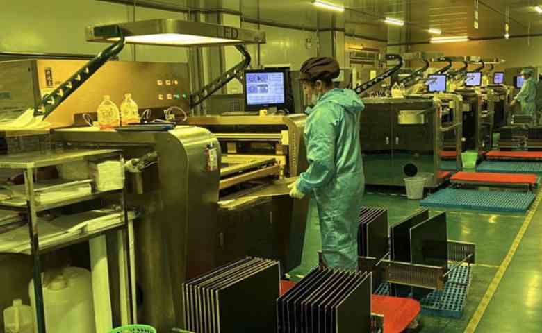
- Automated Production Lines:
- Automated etching machines (Koh Young KY-3030) process 10 panels per hour — 5× faster than manual lines.
- Robot-assisted solder mask application ensures uniform coverage in 2 minutes per panel (vs. 10 minutes manual).
- In-Stock Material Inventory:
20,000+ square meters of FR4, polyimide, and LCP substrates are stocked on-site — eliminating 3–5 days of material sourcing delays for standard prototypes.
Real-World Impact
A consumer electronics startup needed a prototype for a new wireless earbud charging case to meet a CES demo deadline:
- ShwayPCB’s rapid-turn production delivered 10 4-layer prototypes in 48 hours (vs. the 7 days quoted by competitors).
- The prototype validated the charging circuit design, enabling the demo and securing $2M in investor funding.
Explore rapid-turn production at rapid-turn prototype PCB production.
Core Element 4: Quality-Validated Prototype PCB Manufacturing – Avoid Innovation Killers
Poor quality prototypes waste time and money—quality-validated prototype PCB manufacturing embeds rigorous testing at every stage to ensure boards meet design specs and perform reliably.
Technical Quality Checks
- Pre-Fabrication Design Review:
AI-driven DFM (Design for Manufacturability) tools (Siemens Calibre) flag issues like:
- Trace width/spacing violations (e.g., 0.08mm spacing that risks short circuits).
- Incorrect drill sizes (e.g., 0.2mm hole for a 0.3mm component lead).
- Incompatible material choices (e.g., FR4 for a 150°C operating environment).
This catches 98% of manufacturability issues upfront.
- In-Process Inspection:
- Automated Optical Inspection (AOI): 5μm resolution cameras check for etching defects (e.g., undercut traces), missing holes, and solder mask misalignment.
- Electrical Testing: Flying probe testers verify continuity (≤1Ω resistance) and isolation (≥10MΩ) for 100% of nets — critical for detecting hidden defects like cracked traces.
- Post-Fabrication Validation:
- Thermal Cycling: 50 cycles (-40°C to 85°C) to test substrate and copper bond integrity.
- Humidity Testing: 1000 hours at 85% RH/85°C to check for corrosion (relevant for outdoor prototypes).
- Impedance Testing: Vector Network Analyzer (VNA) validates 50Ω ±2% impedance for high-speed traces.
Real-World Impact
An aerospace startup required a high-reliability prototype for a satellite communication module:
- ShwayPCB’s quality validation included thermal cycling, impedance testing, and X-Ray inspection (for hidden via defects).
- The prototype passed all tests, and the final product achieved 99.9% operational uptime in orbit—no redesigns needed.
Explore quality validation at quality-validated prototype PCB manufacturing.
Core Element 5: Scalable Prototype PCB Fabrication – From Innovation to Production
The best prototype manufacturing doesn’t just build a board—it builds a bridge to production. scalable prototype PCB fabrication ensures prototype processes, materials, and designs align with mass production, eliminating costly reworks.
Technical Scalability Features
- Production-Aligned Panelization:
Prototypes are designed to fit standard production panels (e.g., 300×400mm) — avoiding re-panelization costs (\(500–\)1k) and reducing material waste from 30% to 5%. For example, a 50×70mm prototype is panelized to fit 12 units per production panel.
- Process Consistency:
Prototype manufacturing uses the same equipment and parameters as production:
- Same etching chemistry (alkaline vs. acidic) to ensure copper trace consistency.
- Same solder mask type (LPI) and curing process (UV + thermal) to avoid adhesion issues in production.
- Documentation for Handoff:
ShwayPCB provides a “production readiness package” including:
- Gerber files optimized for production.
- Material specifications (substrate, copper weight, finish).
- Process parameters (etching time, drill speeds, curing temperatures).
Real-World Impact
A smart home company scaled a 10-unit prototype to 10,000-unit production:
- Scalable fabrication ensured the production panels matched the prototype’s design — no rework for panelization.
- Process consistency led to 98.5% production first-pass yield (vs. 85% for non-scalable prototypes), saving $15k in rework.
Explore scalability at scalable prototype PCB fabrication.
ShwayPCB: Powering Innovation Through Prototype PCB Manufacturing
ShwayPCB’s prototype PCB manufacturing services embody all 5 core elements, delivering results that fuel electronic innovation:
- Precision: ±0.02mm etching accuracy, ±5μm drilling precision.
- Material Flexibility: FR4, high-Tg FR4, polyimide, LCP substrates.
- Speed: 3–4 day delivery for standard prototypes, 48-hour expedited service.
- Quality: 99.2% first-pass yield, IPC-A-600 Class 2/3 compliance.
- Scalability: 80% of prototypes require 0 redesigns for production.
Innovation Success Story: A startup developing a portable air quality monitor partnered with ShwayPCB:
- Material Optimization: High-Tg FR4 substrate handled the monitor’s 85°C operating temperature.
- Rapid-Turn Production: 10 prototypes delivered in 3 days, enabling fast iteration.
- Quality Validation: Impedance testing ensured accurate sensor data transmission.
- Scalability: Production-aligned panelization cut scaling time by 4 weeks.
The monitor launched 6 weeks early and captured 18% of the portable air quality market—all thanks to reliable prototype PCB manufacturing.
FAQ: Prototype PCB Manufacturing for Electronic Innovation
1. Is prototype PCB manufacturing more expensive for complex designs (8-layer HDIs, microvias)?
Complex designs cost 20–30% more upfront (e.g., \(250 vs. \)200 for 10 units) but deliver 5× ROI by avoiding rework:
- 8-layer HDIs with microvias require laser drilling (vs. mechanical) — adds \(50 per prototype but eliminates 2–3 re-spins (\)1k–$3k savings).
- ShwayPCB’s scalable fabrication ensures complex prototypes align with production, saving $10k+ in post-prototype redesigns.
2. How long does rapid-turn prototype PCB production take for flexible (polyimide) prototypes?
Flexible prototypes require specialized processing (e.g., laser cutting, flexible solder mask) but still meet fast timelines:
- Standard Lead Time: 4–5 days for 2-layer polyimide prototypes.
- Expedited Service: 72 hours for urgent projects (e.g., investor demos).
ShwayPCB’s in-stock polyimide substrates and automated flexible production lines enable this speed.
3. Can prototype PCB manufacturing support high-frequency designs (5G, Wi-Fi 7)?
Yes—ShwayPCB uses LCP substrates and tight process controls for high-frequency prototypes:
- LCP’s low Df (<0.002 at 10GHz) minimizes signal loss for 5G (28GHz) and Wi-Fi 7 (6GHz) designs.
- Etching accuracy (±0.01mm) ensures impedance control (50Ω ±1%) — critical for high-speed signal integrity.
A 5G base station prototype achieved -1.2dB insertion loss (vs. the -2dB requirement) using these capabilities.
4. What quality standards does prototype PCB manufacturing adhere to?
ShwayPCB follows global industry standards to ensure reliability:
- IPC-A-600 Class 2: For commercial prototypes (e.g., consumer electronics).
- IPC-A-600 Class 3: For high-reliability prototypes (medical, automotive, aerospace).
- ROHS 3: Restricts hazardous substances (lead, mercury) for global market access.
- ISO 9001: Ensures consistent quality management across all processes.
5. Can I use my own design files (Gerbers) for prototype PCB manufacturing?
Yes—ShwayPCB accepts Gerbers in RS-274X format (industry standard) and provides a free DFM review to optimize files:
- File Requirements: Include all layers (top/bottom copper, solder mask, silkscreen, drill files).
- DFM Review: Flags issues like trace spacing violations or incorrect drill sizes within 24 hours.
A startup’s Gerber files had 0.08mm trace spacing — DFM review recommended widening to 0.12mm, avoiding short circuits in testing.
6. How does scalable prototype PCB fabrication help with production ramp-up?
Scalable fabrication ensures a seamless transition from prototype to production:
- Panelization: Prototype panels match production sizes (e.g., 300×400mm) — no re-design for panelization.
- Process Alignment: Same etching, drilling, and solder mask processes are used — production FPY matches prototype FPY (98%+).
- Documentation: Production teams receive optimized Gerbers and process parameters — ramp-up takes 3 days (vs. 2 weeks for non-scalable prototypes).
Partner with ShwayPCB for Innovation-Driven Prototype PCB Manufacturing
Prototype PCB manufacturing is the foundation of electronic innovation—and ShwayPCB’s technical expertise in precision, material optimization, speed, quality, and scalability ensures your prototypes turn bold ideas into market-ready products. Whether you’re designing a wearable, 5G module, or industrial sensor, their services reduce risk, accelerate iteration, and align with your long-term production goals.
To request a prototype quote, submit your design files for a free DFM review, or learn how to tailor prototype PCB manufacturing to your innovation, contact ShwayPCB at yuan@shwaypcb.com.

Copyright © 2005-2025 ShwayPCB : PCB Fabrication and Assembly Manufacturer. All Rights Reserved. POWERED BY UEESHOP


Copyright © 2005-2025 ShwayPCB : PCB Fabrication and Assembly Manufacturer. All Rights Reserved. POWERED BY UEESHOP