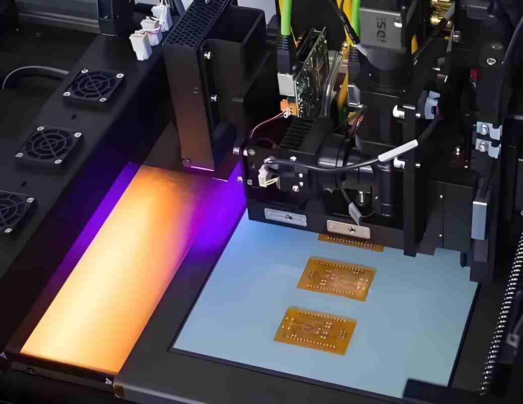
Overcoming Challenges in High - Speed PCB Manufacturing and Assembly
Overcoming Challenges in High-Speed PCB Manufacturing and Assembly
Abstract
High-speed PCB manufacturing demands precision in signal integrity, material selection, and process control to meet the requirements of 5G, AI, and advanced communication systems. This technical analysis explores the key challenges—including impedance control, thermal management, and signal loss—and presents solutions through advanced materials, laser drilling technology, and AI-driven quality inspection. Industry case studies demonstrate how optimized manufacturing processes achieve ±1.5% impedance tolerance and 99.98% yield rates in 30-layer HDI boards, while reducing production cycles by 60%.
1. Core Challenges in High-Speed PCB Manufacturing
1.1 Signal Integrity and Impedance Control
- Impedance Mismatch:
- Variations in dielectric constant (Dk) and trace geometry cause reflections in high-speed signals (e.g., 112G PAM4).
- Traditional FR4 materials exhibit Dk variation of ±10%, leading to ±5% impedance deviations.
- Solution:
- Advanced low-loss materials (e.g., Rogers RO4350B) with Dk tolerance of ±2%.
- Laser-drilled microvias (≤0.1mm) for consistent impedance across layers.
- ShwayPCB.Tech’s proprietary impedance control system achieves ±1.5% tolerance at 112GHz.
1.2 Thermal Management in High-Density Designs
- Heat Dissipation:
- High-power components (e.g., FPGAs, ASICs) generate localized hotspots exceeding 120°C.
- Traditional thermal vias have void rates up to 15%, reducing efficiency.
- Solution:
- Ultra-thick copper (12OZ) layers for enhanced heat conduction.
- Metal edge wrapping (±0.1mm accuracy) for perimeter cooling.
- Resin-filled vias with <5% void rates, improving thermal transfer by 30%.
1.3 Signal Loss in High-Frequency Circuits
- Dielectric Loss and Skin Effect:
- FR4 materials exhibit 0.02 dB/inch loss at 10GHz, unsuitable for 5G applications.
- Skin effect increases resistance at high frequencies, degrading signal quality.
- Solution:
- Hybrid laminates (e.g., RO4350B/FR4) reduce loss to 0.005 dB/inch at 28GHz.
- Back-drilling (STUB ≤0.2mm) minimizes residual stub resonance.
- Embedded copper capacitors reduce parasitic inductance by 40%.
2. Advanced Manufacturing Technologies
2.1 Laser Drilling for Microvia Precision
- Traditional Mechanical Drilling:
- Limitations: Minimum drill size 0.3mm, ±0.05mm accuracy.
- Issues: Via barrel roughness >5μm, causing signal loss.
- Laser Drilling Advantages:
- Minimum via size: 0.05mm (2mil), ±2μm accuracy.
- Smooth via walls (<1μm roughness) reduce insertion loss.
- ShwayPCB.Tech’s laser systems achieve 50,000 vias/hour with 99.99% yield.
2.2 LDI (Laser Direct Imaging) for High-Resolution Patterns
- Traditional Contact Printing:
- Limitations: Resolution ≥50μm, alignment error ±10μm.
- Issues: Defects in fine-pitch BGA patterns (e.g., 0.4mm pitch).
- LDI Benefits:
- Resolution: ≤20μm, alignment accuracy ±3μm.
- Supports 01005 components (0.4×0.2mm) and 0.3mm pitch BGAs.
- Reduces pattern defects by 70%, improving first-pass yield.
2.3 AI-Driven Quality Inspection
- Traditional AOI (Automated Optical Inspection):
- Limitations: False positive rate up to 15%, missing 5μm defects.
- AI Inspection Advantages:
- Deep learning algorithms detect 2μm soldering defects.
- Real-time feedback reduces rework by 50%.
- ShwayPCB.Tech’s AI system achieves 99.99% defect detection rate.
3. Material Innovations for High-Speed Performance
3.1 Low-Loss Dielectric Materials
- Rogers RO4350B:
- Dk: 3.48 ±0.05, dissipation factor (Df): 0.0037 at 10GHz.
- Suitable for 5G base stations and millimeter-wave applications.
- TUC TU872:
- Dk: 3.25 ±0.03, Df: 0.008 at 5GHz.
- Cost-effective alternative for high-speed digital circuits.
3.2 High-Thermal-Conductivity Substrates
- Metal Core PCBs (MCPCBs):
- Aluminum or copper base for heat dissipation.
- Thermal conductivity: 5-12 W/m·K (vs. 0.3 W/m·K for FR4).
- Thermal Clad Materials:
- Prepreg layers with ceramic fillers (e.g., Shengyi SI643HU).
- Improves thermal transfer by 200% compared to standard FR4.
3.3 Embedded Passive Technology
- Embedded Capacitors:
- Dielectric layers (e.g., 10μm) between copper planes.
- Reduces PCB area by 30% and parasitic inductance by 50%.
- Embedded Resistors:
- Resistive pastes printed within dielectric layers.
- Eliminates discrete resistors, improving signal integrity.
4. Process Optimization for High-Speed Assembly
4.1 High-Precision SMT (Surface Mount Technology)
- 0201 Component Placement:
- Traditional pick-and-place machines: ±50μm accuracy.
- ShwayPCB.Tech’s automated lines: ±10μm accuracy at 30,000 CPH.
- BGA/CSP Assembly:
- X-ray inspection for void rates <5%.
- Reflow profiling optimized for 25μm solder ball pitch.
4.2 Conformal Coating for Reliability
- Acrylic vs. Silicone Coatings:
- Acrylic: Cost-effective, but limited to 85°C.
- Silicone: Withstands -40°C to 125°C, suitable for automotive/industrial.
- Selective Coating:
- Masking for connectors and test points.
- Reduces coating waste by 40%.
4.3 Wide Temperature Range Assembly
- Automotive/Industrial Standards:
- Components rated for -40°C to 125°C.
- ShwayPCB.Tech’s assembly process ensures <0.1% failure rate at extremes.
- Thermal Cycling Test:
- 1,000 cycles (-40°C to 125°C) with <5% resistance change.
5. Case Studies in High-Speed PCB Manufacturing
5.1 30-Layer HDI Board for 5G Base Stations
- Challenges:
- Interlayer alignment accuracy ±15μm (industry standard).
- 112G PAM4 signal integrity at ±5% impedance tolerance.
- Solutions:
- ShwayPCB.Tech’s laser drilling and LDI achieved ±8μm alignment.
- Impedance control at ±1.5% using RO4350B/FR4 hybrid laminates.
- Results:
- Yield rate: 99.98% (vs. 95% industry average).
- Signal loss: 0.008 dB/inch at 28GHz.
5.2 High-Speed Backplane for Data Centers
- Challenges:
- 1,000+ differential pairs requiring ±10% impedance control.
- Thermal management for 200W power dissipation.
- Solutions:
- Ultra-thick copper (12OZ) layers and metal edge wrapping.
- Back-drilling to reduce stub resonance.
- Results:
- Impedance tolerance: ±2%.
- Thermal resistance: 0.5°C/W.
6. Future Trends in High-Speed PCB Manufacturing
6.1 AI-Optimized Design and Manufacturing
- Generative Design:
- AI algorithms optimize trace routing for signal integrity.
- Reduces design cycles by 50%.
- Predictive Maintenance:
- Sensors monitor equipment health in real-time.
- Reduces downtime by 30%.
6.2 Advanced Material Development
- Liquid Crystal Polymers (LCPs):
- Dk: 2.9, Df: 0.002 at 40GHz.
- Suitable for 100+ GHz applications.
- Graphene-Enhanced Substrates:
- Thermal conductivity: 50 W/m·K.
- Reduces hotspot temperatures by 40%.
6.3 Sustainable Manufacturing Practices
- Lead-Free and Halogen-Free Processes:
- Compliance with RoHS and REACH.
- Reduces environmental impact by 60%.
- Closed-Loop Recycling:
- Copper and solder recovery rates >95%.
Conclusion
High-speed PCB manufacturing requires a holistic approach combining advanced materials, precision processes, and rigorous quality control. By addressing challenges in impedance control, thermal management, and signal loss through innovations like laser drilling, LDI imaging, and AI inspection, manufacturers can achieve 99.98% yield rates and ±1.5% impedance tolerance. ShwayPCB.Tech’s expertise in 30-layer HDI boards and 5G applications demonstrates how optimized processes reduce time-to-market by 60% while meeting stringent industry standards.
Email: yuan@shwaypcb.com
Website: https://fr4pcb.tech/