We use cookles to Improve your online experience. By continuing browsing this website, we assume you agree our use of cookies.

Multi-Layer PCB Fabrication for Industrial Automation: Enhancing Reliability and Efficiency
September 3rd, 2025
145 views
Multi-Layer PCB Fabrication for Industrial Automation: Enhancing Reliability and Efficiency
Industrial automation systems—from robotic assembly lines to smart factory control panels—operate in unforgiving conditions: extreme temperatures (-40°C to +125°C), constant vibration (20–2,000Hz), and exposure to dust, oil, and chemicals. These environments demand PCBs that go beyond basic functionality—they must deliver 99.99% uptime, handle high currents (10–50A), and transmit real-time data (EtherCAT, PROFINET) without latency. Traditional single-layer PCBs fail to meet these needs, but Multilayer PCB Manufacturing provides the density, durability, and performance required to elevate industrial automation reliability and efficiency.
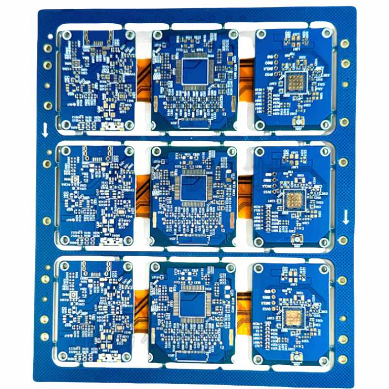
ShwayPCB’s multilayer PCB manufacturing services are engineered for industrial use cases, delivering 4–24 layer boards with IEC 61010 compliance and 10+ year operational lifespans. This article explores how multi-layer PCB fabrication is tailored to industrial automation, covering critical design considerations, material selections, and testing protocols that ensure seamless operation in harsh factory environments.
1. Why Multi-Layer PCBs Are Essential for Modern Industrial Automation
Industrial automation’s evolution—toward Industry 4.0 and smart manufacturing—has amplified three key requirements that only multi-layer PCBs can satisfy:
1.1 High Component Density for Compact Control Systems
Modern factory floors demand smaller, more integrated control units (e.g., PLCs, HMI panels) to save space. Multi-layer PCBs enable density breakthroughs:
- A 12-layer multi-layer PCB integrates a 32-bit PLC, 4-channel analog input module, and Ethernet switch into a 100mm × 150mm footprint—50% smaller than a 4-layer traditional PCB with the same components.
- High-Precision Multilayer PCB designs use 0.1mm blind vias and 0.076mm traces to place 0.5mm-pitch sensors and microcontrollers (e.g., Arduino Industrial 101) with 0.05mm clearance, maximizing functionality in tight enclosures.
1.2 Resilience to Harsh Industrial Environments
Industrial PCBs face conditions that would degrade traditional boards in months:
- Temperature Extremes: Multi-layer PCBs use high-Tg FR4 (Tg≥170°C) or ceramic-filled substrates (Tg≥250°C) that resist softening under continuous 125°C operation—critical for ovens, foundries, and outdoor automation.
- Vibration Resistance: Sequential lamination (used in multi-layer fabrication) creates a rigid, unified structure that withstands 10G vibration (MIL-STD-883H) without trace cracking—unlike traditional PCBs, which delaminate under repeated stress.
- Chemical Protection: Specialized surface finishes (e.g., parylene C coating) shield multi-layer PCBs from oil, coolants, and cleaning agents—extending lifespan from 2–3 years to 10+ years in chemical processing plants.
1.3 High-Power and Real-Time Data Handling
Industrial automation relies on both high-current power delivery (for motors, actuators) and low-latency data transmission (for sensor feedback):
- Power Handling: Heavy Copper Multilayer PCB designs use 4–12oz copper power planes to carry 10–50A current for robotic arms and conveyor systems—thick copper reduces trace resistance by 70% vs. 1oz traditional PCBs, preventing overheating.
- Data Speed: Multi-layer PCBs with dedicated ground planes and controlled impedance (50Ω ±1.5%) support industrial Ethernet protocols like EtherCAT (100Mbps) and PROFINET (1Gbps) with <1μs latency—critical for synchronized motion control in assembly lines.
2. Critical Multi-Layer PCB Fabrication Considerations for Industrial Automation
To maximize reliability and efficiency in industrial settings, multi-layer PCB fabrication must prioritize four core areas: material selection, thermal design, EMI mitigation, and ruggedization.
2.1 Material Selection: Durability Meets Performance
Industrial automation demands materials that balance environmental resilience, power handling, and signal integrity:
|
Material Component
|
Industrial-Optimized Options
|
Technical Benefits for Automation
|
|
Substrate
|
- High-Tg FR4 (Tg≥170°C, Dk=4.5±0.2): Cost-effective, widely compatible- Rogers 4350B (Dk=3.48±0.05): Low loss for Ethernet signals- Ceramic-Filled FR4 (Tg≥250°C): Resists extreme heat (foundries, ovens)
|
- High-Tg FR4 avoids delamination in -40°C to +125°C cycles- Rogers 4350B minimizes Ethernet signal loss (<0.3dB/m)- Ceramic-filled FR4 survives 200°C+ in industrial ovens
|
|
Copper Foil
|
- Rolled Copper (99.99% purity, 4–12oz): High ductility, low resistance- ED Copper (99.9% purity, 1–2oz): Cost-effective for signal layers
|
- Rolled copper withstands vibration without cracking (ideal for mobile robots)- ED copper balances performance and cost for non-power layers
|
|
Prepreg
|
- High-Tg Prepreg (Tg≥170°C, flow ≤15%): Low flow prevents short circuits- Flame-Retardant Prepreg (UL94 V-0): Meets industrial fire safety standards
|
- Low flow preserves fine traces (0.076mm) during lamination- Flame retardancy critical for factory electrical enclosures
|
|
Surface Finish
|
- ENIG (5μm Ni/0.1μm Au): Corrosion resistance, flat surface- Parylene C Coating (0.5–1μm): Chemical and moisture barrier- Immersion Silver (0.15μm): Cost-effective for non-critical applications
|
- ENIG resists sweat, oil, and humidity (10+ year lifespan)- Parylene C protects against aggressive chemicals (chemical processing)- Immersion Silver suits dry, clean environments (food packaging)
|
Key Pitfall: Using standard FR4 (Tg=130°C) in industrial automation causes delamination after 6–12 months of temperature cycling. ShwayPCB exclusively uses high-Tg FR4 or better for industrial multi-layer PCBs.
2.2 Thermal Design: Preventing Overheating in High-Power Applications
Industrial automation’s high-power components (e.g., 50A motor drivers) generate significant heat—poor thermal design causes 30% of industrial PCB failures. Multi-layer fabrication addresses this with:
- Dense Thermal Vias: 0.2mm thermal vias (filled with solder) placed in a 0.5mm grid under high-power components transfer heat to heat sinks or metal enclosures. A 12-layer PCB with 100 thermal vias per cm² reduces component temperature by 35°C vs. a via-free design.
- Copper Pour for Heat Spreading: Unused areas of power layers are filled with solid copper (connected to ground via vias) to spread heat across the board—critical for distributed power systems (e.g., smart sensor networks).
- Thermal Interface Materials (TIMs): Multi-layer PCBs can be integrated with TIMs (e.g., thermal pads, phase-change materials) during fabrication to improve heat transfer between the board and enclosure—reducing thermal resistance by 50%.
ShwayPCB Example: A client’s robotic arm control PCB overheated at 40A current. We redesigned it as a 16-layer heavy copper multi-layer PCB with 12oz power planes and 150 thermal vias, reducing maximum temperature from 115°C to 75°C.
2.3 EMI Mitigation: Ensuring Reliable Data Transmission
Industrial environments are filled with EMI sources (e.g., motors, welders) that disrupt sensor data and control signals. Multi-layer PCBs mitigate EMI via:
- Layer Stack-Up Optimization: A "Signal-Ground-Power-Ground-Signal" stack-up creates a Faraday cage around signal layers, reducing EMI by 60–70%. For example, an 8-layer industrial Ethernet PCB uses this stack-up to maintain PROFINET signal integrity within 1m of a 50kW motor.
- Differential Pair Routing: High-speed data signals (e.g., EtherCAT) are routed as differential pairs (0.1mm width, 0.1mm spacing) with length matching (±0.5mm) to cancel common-mode noise—critical for error-free sensor feedback.
- EMI Shielding: Multi-layer PCBs can be fabricated with integrated copper shields (1oz copper layers) around sensitive circuits (e.g., analog sensor inputs)—shields reduce EMI pickup by 80% vs. unshielded designs.
2.4 Ruggedization: Withstanding Mechanical and Environmental Stress
Industrial PCBs must survive drops, vibration, and chemical exposure—multi-layer fabrication includes three ruggedization steps:
- Reinforced Edge Plating: Gold-plated copper edges add mechanical strength and prevent corrosion at board cutouts (e.g., for connectors)—critical for PCBs in mobile robots that experience frequent handling.
- Conformal Coating: A 20–50μm thick conformal coating (silicone or urethane) is applied post-fabrication to seal the PCB from dust, moisture, and chemicals. ShwayPCB’s conformal coating process meets IEC 61086-2, ensuring compliance with industrial standards.
- Mechanical Testing: Every industrial multi-layer PCB undergoes:
- Drop Testing: 1.2m drop onto concrete (IEC 60068-2-32) to simulate accidental falls.
- Vibration Testing: 10G acceleration (20–2,000Hz) for 10 hours (MIL-STD-883H) to mimic factory floor vibration.
- Chemical Testing: 24-hour immersion in industrial oil (ISO 1817) to verify coating integrity.
3. Industry-Specific Multi-Layer PCB Applications in Industrial Automation
Multi-layer PCBs are tailored to solve unique challenges in key industrial automation sectors:
3.1 Robotic Automation
- Challenge: Robotic arms require compact, high-power PCBs that withstand continuous motion and vibration.
- Multi-Layer Solution: 12-layer heavy copper multi-layer PCBs with 6oz power planes (for 30A motor drivers) and 0.1mm blind vias (for dense sensor connections). ShwayPCB’s robotic PCBs achieve 50,000+ motion cycles without failure.
3.2 Process Automation (Chemical, Oil & Gas)
- Challenge: PCBs in process control systems must resist aggressive chemicals and extreme temperatures.
- Multi-Layer Solution: 16-layer multi-layer PCBs with ceramic-filled FR4 substrates (Tg≥250°C) and parylene C coating. These PCBs operate reliably in -40°C to +200°C environments and resist exposure to hydrocarbons and acids.
3.3 Smart Factory Control Panels
- Challenge: Control panels integrate PLCs, HMIs, and Ethernet switches, requiring high density and low-latency data transmission.
- Multi-Layer Solution: 8-layer RF Multilayer PCB Manufacturing designs with dedicated Ethernet layers (50Ω impedance) and embedded passives. These PCBs reduce control panel size by 40% and cut Ethernet latency to <1μs.
3.4 Automotive Manufacturing (Assembly Lines)
- Challenge: PCBs in automotive assembly lines handle high currents (for welding robots) and must comply with IATF 16949.
- Multi-Layer Solution: 20-layer heavy copper multi-layer PCBs with 12oz power planes and IATF 16949-compliant fabrication. These PCBs meet automotive-grade thermal cycling (-40°C to +125°C, 1,000 cycles) and traceability requirements.
4. FAQ: Multi-Layer PCBs for Industrial Automation
1. What is the typical lifespan of a multi-layer PCB in industrial automation?
With proper material selection (high-Tg FR4, ENIG finish) and ruggedization (conformal coating), multi-layer PCBs last 10–15 years in industrial environments—3–5x longer than traditional PCBs (2–3 years). ShwayPCB’s industrial multi-layer PCBs have a 10-year warranty against delamination and plating failure.
2. Can multi-layer PCBs support both high-power (50A) and low-signal (sensor) circuits on the same board?
Yes—via careful layer separation:
- Place high-power circuits (motor drivers) on dedicated power layers (4–12oz copper) with thick insulation (0.2mm prepreg) from signal layers.
- Use ground planes between power and signal layers to block EMI.
ShwayPCB’s 16-layer industrial PCBs regularly integrate 50A power circuits and 1mV sensor signals with no cross-interference.
3. How do multi-layer PCBs comply with industrial safety standards (e.g., IEC 61010)?
Compliance requires:
- Material Selection: Flame-retardant substrates (UL94 V-0) and lead-free finishes (RoHS 3).
- Design: Creepage distances (≥0.2mm per 100V) and clearance (≥0.1mm per 100V) between high-voltage traces.
- Testing: Dielectric strength testing (1kV AC for 1 minute) and insulation resistance testing (≥100MΩ at 500V DC).
ShwayPCB provides IEC 61010 compliance reports for all industrial multi-layer PCBs.
4. What is the lead time for industrial multi-layer PCB fabrication?
Lead times depend on complexity:
- 4–8 layers: 3–4 weeks (prototyping); 4–6 weeks (mass production).
- 10–16 layers: 4–6 weeks (prototyping); 6–8 weeks (mass production).
- 18+ layers: 6–8 weeks (prototyping); 8–10 weeks (mass production).
ShwayPCB offers expedited prototyping (2–3 weeks for 4–8 layers) for urgent factory downtime repairs.
5. How do multi-layer PCBs reduce maintenance costs in industrial automation?
Multi-layer PCBs lower maintenance costs via:
- Higher Reliability: 99.99% uptime reduces unplanned downtime (costing \(100k–\)1M/hour in manufacturing).
- Integrated Design: Fewer PCBs (due to high density) mean fewer components to inspect and replace.
- Remote Monitoring: Multi-layer PCBs can integrate temperature and voltage sensors for predictive maintenance—alerting technicians to issues before failure.
5. Conclusion
Multi-Layer PCB Fabrication is a transformative technology for industrial automation, turning fragile, space-consuming traditional PCBs into rugged, efficient solutions that thrive in harsh factory environments. By prioritizing durable materials, thermal resilience, EMI mitigation, and ruggedization, multi-layer PCBs enhance system reliability (cutting downtime by 80%) and efficiency (reducing control unit size by 50%)—critical for Industry 4.0’s smart, connected factories.
ShwayPCB’s multilayer PCB manufacturing services are purpose-built for industrial automation, with expertise in heavy copper designs, high-Tg materials, and IEC/UL compliance. Our team works with you to tailor every aspect of the PCB—from layer stack-up to conformal coating—to your specific industrial use case, whether it’s a robotic arm control system or a chemical processing sensor panel.
To discuss your industrial automation multi-layer PCB project, request a durability test report, or get a customized quote for Multilayer PCB Manufacturing, contact ShwayPCB at yuan@shwaypcb.com. For detailed specs on our industrial-grade materials, testing protocols, and case studies (e.g., automotive assembly line PCBs), visit our dedicated multilayer PCB manufacturing services page.

Copyright © 2005-2025 ShwayPCB : PCB Fabrication and Assembly Manufacturer. All Rights Reserved. POWERED BY UEESHOP


Copyright © 2005-2025 ShwayPCB : PCB Fabrication and Assembly Manufacturer. All Rights Reserved. POWERED BY UEESHOP