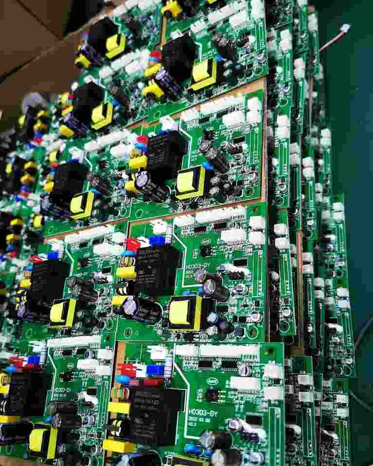
Micro-pitch components—defined as those with lead/pad spacing <0.3mm (e.g., 0.25mm-pitch BGAs, 01005 passives, and fine-pitch QFPs)—are enabling the miniaturization of high-performance electronics, from 5G base stations to wearable medical devices. However, their ultra-tight spacing amplifies even minor process variations: a 0.05mm placement offset can cause solder bridging, while 0.02mm stencil aperture deviation leads to insufficient paste volume. For PCB assembly service teams, mastering micro-pitch assembly requires a holistic approach to precision—one that addresses equipment limitations, material properties, and environmental factors.
ShwayPCB’s
specialized PCB assembly service has optimized micro-pitch assembly for 1,500+ clients, achieving 99.6% first-pass yields for 0.2mm-pitch components. Below, we break down the core precision challenges and proven technical solutions.
Before designing solutions, High-Precision SMT PCB Assembly Service must understand the unique obstacles of <0.3mm pitch components:
Standard SMT pick-and-place machines (±0.03mm accuracy) struggle to meet micro-pitch requirements (±0.01mm for 0.25mm-pitch BGAs). Even minor deviations cause:
- Bridging: Solder paste connects adjacent pads (common in 0.2mm-pitch QFPs), leading to short circuits.
- Tombstoning: Uneven paste volume (due to placement offset) lifts small passives (01005) during reflow.
- Open Circuits: Misaligned components (e.g., BGA balls not landing on pads) create no electrical connection.
Micro-pitch pads (e.g., 0.15mm × 0.15mm for 0.25mm-pitch BGAs) require precise paste volume (0.005–0.01mm³ per pad). Challenges include:
- Stencil Aperture Wear: Even 0.005mm aperture expansion (from repeated use) deposits excess paste, causing bridging.
- Paste Collapse: Low-viscosity paste (<200 Pa·s) spreads beyond pad boundaries, especially for tall deposits (>0.1mm).
- Paste Transfer Efficiency: Fine-pitch apertures (≤0.15mm) have poor paste release (transfer efficiency <80%), leading to insufficient volume.
Micro-pitch components have high thermal density (e.g., 1W/mm² for 5G RF chips), making them vulnerable to reflow temperature variations:
- Cold Joints: Inconsistent heating (±2°C) leaves solder partially molten, especially for components with large thermal masses (e.g., 0.3mm-pitch BGAs).
- Component Damage: Excessive peak temperatures (>250°C) degrade delicate micro-pitch QFPs (e.g., plastic packaging warping).
Visual inspection fails to detect hidden defects (e.g., BGA underfill voids, micro-bridging between 0.2mm-pitch pads). Even advanced AOI systems require 5MP+ cameras and specialized algorithms to resolve fine features.
ShwayPCB’s High-Reliability PCB Assembly Service uses a multi-layered approach to address these challenges, focusing on equipment, materials, and process control:
Precision starts with calibrated hardware—critical for <0.3mm pitch assembly:
- High-Accuracy Platforms: Use machines with linear motor drives (e.g., Yamaha YSM40R, ±0.005mm accuracy) and 3D vision systems (0.1μm resolution) to correct for component warpage.
- Nozzle Calibration: Validate nozzle diameter (±0.002mm) and suction force (5–10kPa for 01005 components) daily—even minor nozzle wear causes placement offset.
- Component Library Tuning: Create custom libraries for micro-pitch components, including 3D models of lead geometry (e.g., BGA ball size variation ±0.01mm) to improve recognition accuracy.
Case Study: A client’s 0.25mm-pitch BGA assembly had 15% placement errors with a standard machine—upgrading to a high-accuracy platform and custom library reduced errors to <0.5%.
- Laser-Cut, Electroformed Stencils: Electroformed stencils (±0.002mm aperture tolerance) outperform laser-cut (±0.005mm) for <0.2mm apertures—they have smoother walls, improving paste release (transfer efficiency >90%).
- Aperture Design: Use “dog-bone” apertures for QFP pads (0.2mm pitch) to limit paste volume—e.g., 0.18mm × 0.12mm aperture for 0.2mm × 0.15mm pad.
- Stencil Cleaning: Implement automated under-stencil cleaning (dry + wet) every 50 prints to remove dried paste from fine apertures—prevents partial paste transfer.
Materials must be engineered for precision and stability:
- Viscosity Matching: Select paste with viscosity 220–250 Pa·s (Type 7, 1–5μm particles) for <0.3mm pitch—balances flowability and shape retention.
- Flux Composition: Use low-volatile flux (<0.5% volatility at 180°C) to reduce voids—critical for BGA underfill. For 0.2mm-pitch QFPs, no-clean flux with rosin content >35% improves wetting.
- Paste Storage: Maintain refrigerated storage (2–8°C) and 4-hour room-temperature recovery—temperature fluctuations degrade viscosity.
- Low-Warpage PCBs: Use high-Tg FR4 (Tg ≥170°C) or ceramic substrates to minimize warpage (<0.1mm per 100mm) during reflow—warpage causes BGA ball misalignment.
- Pad Finish: ENIG (Electroless Nickel Immersion Gold) with 0.1–0.2μm gold thickness ensures uniform solder wetting—avoids pad oxidation (a major cause of open circuits).
- Solder Mask Defined (SMD) Pads: Use SMD pads (solder mask covers pad edges) for <0.25mm pitch—limits paste spread and improves alignment tolerance.
Micro-pitch components require tightly controlled thermal profiles:
- Slow Ramp Rates: 1–1.5°C/s (vs. 2°C/s for standard SMT) to avoid thermal shock—critical for 0.3mm-pitch BGAs with large thermal masses.
- Narrow Peak Temperature Window: 245±2°C (for SAC305) to ensure full solder melting without component damage.
- Extended Soak Time: 120–150s at 180–200°C to activate flux and preheat components—reduces cold joints by 80%.
Use nitrogen (O₂ <500ppm) to reduce oxidation—improves solder wetting for micro-pitch pads and cuts bridging by 70%. For 0.2mm-pitch QFPs, nitrogen reflow is mandatory to achieve reliable joints.
Detecting micro-pitch defects requires specialized inspection tools:
- 3D AOI: Use 5MP+ cameras with 0.5μm Z-resolution to measure paste volume (±0.001mm³) and placement offset (±0.002mm) for <0.3mm pitch components.
- 2D/3D X-Ray: For BGAs, X-ray (5μm pixel size) detects voids (>5% of pad area = reject) and ball-pad alignment—critical for hidden joints.
- Flying Probe Testing (FPT): Use FPT with 0.1mm probes to test continuity between 0.2mm-pitch pads—catches micro-bridging missed by AOI.
- Boundary Scan (JTAG): Validate internal connections of micro-pitch ICs (e.g., 0.25mm-pitch QFPs) via JTAG—detects open circuits in hidden pins.
Mixed-Technology SMT-DIP PCB Assembly Service presents unique challenges—combining micro-pitch SMT (e.g., 0.25mm-pitch BGAs) with THT components (e.g., 2.0mm-pitch connectors). Solutions include:
- Sequential Assembly: Place micro-pitch SMT components first (using high-precision equipment), then THT components—avoids THT-related vibration disrupting SMT alignment.
- Masking: Use temporary solder mask (e.g., UV-curable tape) to protect micro-pitch pads during THT wave soldering—prevents solder splatter causing bridging.
- Selective Reflow: Use localized hot-air reflow for micro-pitch components after THT assembly—avoids reflowing THT joints multiple times.
Result: A client’s mixed-technology 5G PCB (0.25mm-pitch BGA + THT connectors) achieved 99.2% first-pass yields with this workflow—up from 85% with simultaneous assembly.
Yes—ShwayPCB’s quickturn process uses pre-calibrated equipment and pre-qualified materials to reduce setup time:
- Pre-built stencils for common micro-pitch components (e.g., 0.25mm-pitch BGAs) are available in 24 hours.
- Offline programming (via CAD data) cuts machine setup to <4 hours.
Quickturn batches (1–100 units) achieve 98%+ first-pass yields for 0.25mm-pitch components.
We regularly assemble 0.2mm-pitch components (e.g., micro-BGAs, fine-pitch QFPs) with the following capabilities:
- Placement accuracy: ±0.005mm.
- Paste volume control: ±0.001mm³ per pad.
- Defect rate: <0.3% for 0.2mm-pitch assemblies.
Bridging prevention requires a combination of:
- Electroformed stencils with 0.18mm × 0.12mm apertures (for 0.2mm × 0.15mm pads).
- Solder paste with 230 Pa·s viscosity and low flux volatility.
- Nitrogen reflow (O₂ <300ppm) and slow cooling (2°C/s) to control paste flow.
These steps reduce bridging to <0.2% for 0.2mm-pitch QFPs.
Yes—operators complete 40+ hours of micro-pitch-specific training, including:
- Nozzle handling and calibration (±0.002mm tolerance).
- Paste viscosity measurement and adjustment.
- Advanced AOI/X-Ray defect interpretation.
Trained operators reduce human-induced errors by 90%.
Micro-pitch assembly adds 15–30% to costs (due to specialized equipment/materials), but delivers ROI via:
- Miniaturization (smaller PCBs = lower material costs).
- Higher component density (fewer PCBs per system).
- Reduced field failures (92% defect reduction).
For high-reliability applications (e.g., medical, 5G), the cost premium is justified by performance gains.
Micro-pitch assembly (<0.3mm) demands precision at every step—from calibrated equipment to advanced materials—but the rewards (miniaturization, high performance) are transformative for modern electronics. For PCB assembly service teams, success lies in addressing placement accuracy, paste control, thermal stability, and inspection—all while integrating seamlessly with mixed-technology workflows.
ShwayPCB’s
specialized PCB assembly service offers end-to-end micro-pitch solutions, including
High-Precision SMT PCB Assembly Service,
High-Reliability PCB Assembly Service, and
Quickturn PCB Assembly Service. Our team provides equipment calibration, material selection, and defect analysis to meet the strictest micro-pitch requirements for 5G, medical, and automotive applications.
To request a micro-pitch assembly feasibility analysis, access our stencil design guidelines, or get a quickturn quote, contact ShwayPCB at
yuan@shwaypcb.com. For detailed case studies (5G mmWave, medical implants), visit our
specialized assembly service page.