IoT Device PCB Assembly: Partnering with Low-Volume & High-Mix Experts
IoT Device PCB Assembly: Partnering with Low-Volume & High-Mix Experts
Introduction
The Internet of Things (IoT) has revolutionized the way we interact with technology, connecting a vast array of devices to the internet and enabling seamless data exchange. From smart home appliances and wearable fitness trackers to industrial sensors and autonomous vehicles, IoT devices are transforming industries and enhancing our daily lives. At the heart of these innovative devices lies the Printed Circuit Board (PCB), a critical component that facilitates the electrical connections and functionality of the device. For IoT device manufacturers, especially those operating in low-volume and high-mix production environments, finding the right PCB assembly partner is essential to ensure high-quality, reliable, and cost-effective solutions. In this article, we will explore the unique challenges of IoT device PCB assembly, the benefits of turnkey PCB assembly services, and why choosing a PCB assembly expert in China can be a game-changer for your IoT projects.
Understanding IoT Device PCB Assembly Challenges
Low-Volume Production
Unlike mass-market consumer electronics, many IoT devices are designed for niche applications or specific customer requirements, resulting in low-volume production runs. This presents several challenges for PCB assembly, including:
- Cost Efficiency: Traditional PCB assembly processes are optimized for high-volume production, making it difficult to achieve cost-effective solutions for low-volume orders. Manufacturers must find ways to reduce setup costs, minimize material waste, and streamline production processes to remain competitive.
- Flexibility: Low-volume production requires a high degree of flexibility to accommodate design changes, component substitutions, and customization requests. PCB assembly partners must be able to adapt quickly to these changes without compromising on quality or lead times.
- Inventory Management: Managing inventory for low-volume production can be challenging, as it requires balancing the need to have the right components on hand with the risk of overstocking and incurring additional costs. Effective inventory management strategies are essential to ensure smooth production and minimize delays.
High-Mix Production
In addition to low-volume production, IoT device manufacturers often deal with high-mix production, where a wide variety of different PCB designs and configurations are produced within the same facility. This adds another layer of complexity to PCB assembly, including:
- Equipment Utilization: High-mix production requires PCB assembly equipment that can handle a diverse range of component sizes, shapes, and packaging types. Manufacturers must invest in flexible and versatile equipment to ensure efficient production across different product lines.
- Process Control: Maintaining consistent quality and performance across a high-mix production environment is challenging. PCB assembly partners must implement robust process control measures, such as statistical process control (SPC) and automated inspection systems, to detect and correct any deviations from the desired specifications.
- Skill Requirements: High-mix production demands a skilled workforce with expertise in a wide range of PCB assembly techniques and technologies. Technicians must be able to quickly switch between different product lines and troubleshoot any issues that may arise during the assembly process.
The Benefits of Turnkey PCB Assembly for IoT Devices
Streamlined Supply Chain
Turnkey PCB assembly is a comprehensive solution that encompasses every stage of the PCB assembly process, from component sourcing to final testing and delivery. For IoT device manufacturers, turnkey services offer a streamlined supply chain, eliminating the need to manage multiple suppliers and vendors. This reduces the complexity and administrative burden associated with PCB assembly, allowing manufacturers to focus on their core competencies, such as product design and marketing.
Enhanced Quality Control
A reputable turnkey PCB assembly provider will have a robust quality management system in place, ensuring that every PCB meets the highest quality standards. This includes rigorous component testing, in-process inspection, and final functional testing. By partnering with a turnkey provider, IoT device manufacturers can benefit from their expertise and experience in quality control, reducing the risk of defects and malfunctions in their products.
Faster Time-to-Market
In the fast-paced IoT industry, time-to-market is critical. Turnkey PCB assembly providers can leverage their expertise and resources to accelerate the assembly process, reducing lead times and enabling IoT device manufacturers to bring their products to market more quickly. This is especially important for low-volume and high-mix production, where quick turnaround times can give manufacturers a competitive edge.
Cost Savings
While turnkey PCB assembly services may seem more expensive at first glance, they can actually offer significant cost savings in the long run. By optimizing the assembly process, reducing material waste, and leveraging economies of scale, turnkey providers can offer competitive pricing for low-volume and high-mix production. Additionally, the streamlined supply chain and reduced administrative burden associated with turnkey services can further contribute to cost savings.
PCB Assembly Services for IoT Devices
PCB Assembly
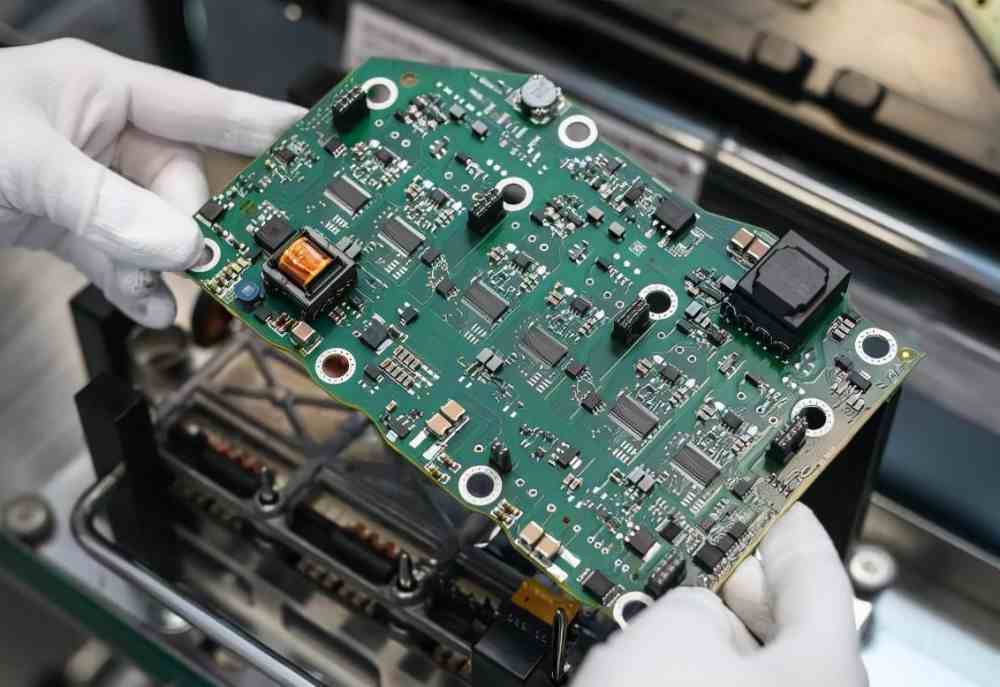
PCB assembly involves the process of mounting electronic components onto a printed circuit board. For IoT devices, PCB assembly requires specialized techniques and equipment to ensure high reliability and performance. Key aspects of IoT device PCB assembly include:
- Component Selection: IoT devices often operate in harsh environments, such as extreme temperatures, humidity, and vibration. Therefore, it is essential to select components that are specifically designed for these conditions and have a long lifespan. Additionally, components should be compatible with the communication protocols used by the IoT device, such as Wi-Fi, Bluetooth, or Zigbee.
- Soldering Techniques: Advanced soldering techniques, such as reflow soldering and selective soldering, should be employed to create strong and reliable connections between components and the PCB. These techniques must be carefully controlled to prevent solder joint defects, such as voids and cracks, which can affect the performance and reliability of the IoT device.
- Cleaning and Conformal Coating: After assembly, the PCBs should be thoroughly cleaned to remove any flux residues or contaminants that could affect their performance. Conformal coating may also be applied to protect the PCBs from moisture, dust, and other environmental factors, extending the lifespan of the IoT device.
- Inspection and Testing: Comprehensive inspection and testing procedures, including visual inspection, automated optical inspection (AOI), and in-circuit testing (ICT), should be carried out to detect any defects or malfunctions before the PCBs are integrated into the IoT device. Functional testing should also be performed to ensure that the IoT device meets the specified performance requirements.
PCB Manufacturing
PCB manufacturing is the process of creating the printed circuit board itself, including designing the layout, etching the copper traces, and drilling holes for component mounting. For IoT devices, PCB manufacturing requires:
- Precision and Accuracy: The PCB layout must be designed with high precision to ensure proper component placement and electrical connectivity. This is especially important for IoT devices, which often have complex circuit designs and small form factors.
- Material Selection: High-quality materials, such as FR-4 with high glass transition temperature (Tg) and low coefficient of thermal expansion (CTE), should be used to ensure the durability and reliability of the PCB under extreme operating conditions. Additionally, materials should be chosen based on their compatibility with the communication frequencies used by the IoT device to minimize signal loss and interference.
- Layer Stackup Design: The layer stackup of the PCB must be carefully designed to optimize signal integrity, power integrity, and thermal management. This may involve using multiple layers of copper and dielectric materials to achieve the desired performance characteristics, especially for IoT devices that require high-speed data transmission or power-hungry components.
- Manufacturing Process Control: Strict process control measures should be implemented during PCB manufacturing to ensure consistency and quality. This includes monitoring and controlling parameters such as etching time, temperature, and pressure, as well as performing regular quality checks throughout the production process.
Quick Turn PCB Assembly
In the dynamic IoT industry, quick turn PCB assembly services are essential for IoT device manufacturers who need to respond quickly to market demands or prototype new designs. Quick turn services typically offer:
- Expedited Production: By optimizing the production process and utilizing advanced equipment, quick turn providers can produce PCB assemblies in a short period, often within a few days or even hours. This allows IoT device manufacturers to accelerate product development and testing, reducing the time-to-market for their products.
- Flexible Scheduling: Quick turn services can accommodate urgent orders and tight deadlines, providing IoT device manufacturers with the flexibility they need to meet changing market conditions and customer requirements. This is especially important for low-volume and high-mix production, where demand can fluctuate rapidly.
- Prototyping and Low-Volume Production: Quick turn providers often offer prototyping and low-volume production services, allowing IoT device manufacturers to test and validate their designs before committing to large-scale production. This helps reduce the risk of design errors and cost overruns, ensuring that the final product meets the desired specifications and performance requirements.
- Quality Assurance: Despite the expedited production process, quick turn providers still maintain strict quality control measures to ensure that the PCB assemblies meet the required standards. This includes comprehensive testing and inspection procedures at every stage of the assembly process, as well as adherence to industry best practices and quality management systems.
Why Choose a PCB Assembly Expert in China for Your IoT Projects
Cost-Effectiveness
China has a well-established electronics manufacturing industry, which allows PCB assembly experts to offer competitive pricing without compromising on quality. The lower labor and production costs in China make it an attractive option for IoT device manufacturers looking to reduce their manufacturing expenses, especially for low-volume and high-mix production.
Advanced Technology and Infrastructure
Chinese PCB assembly providers have invested heavily in advanced technology and infrastructure, enabling them to offer high-quality PCB assembly services. They utilize state-of-the-art equipment, such as high-speed pick-and-place machines, automated optical inspection systems, and X-ray inspection machines, to ensure precision and efficiency in the assembly process. Additionally, many Chinese providers have adopted Industry 4.0 technologies, such as the Internet of Things (IoT) and artificial intelligence (AI), to optimize production and improve quality control.
Skilled Workforce
China has a large pool of skilled engineers and technicians with extensive experience in PCB assembly and manufacturing. These professionals are well-trained in the latest industry standards and technologies, including those specific to IoT device PCB assembly. They can provide valuable expertise and support throughout the entire PCB assembly process, from design review and component selection to production and testing.
Supply Chain Efficiency
China has a well-developed supply chain network, which allows PCB assembly experts to source components quickly and efficiently. This reduces lead times and ensures that IoT device manufacturers can receive their PCB assemblies on time, even for urgent orders. Additionally, many Chinese providers have established relationships with global component suppliers, enabling them to offer a wide range of components at competitive prices, including those that are specifically designed for IoT applications.
Conclusion
The IoT industry presents unique challenges for PCB assembly, especially for low-volume and high-mix production environments. However, by partnering with a turnkey PCB assembly expert that offers comprehensive services, including PCB assembly, manufacturing, and quick turn solutions, IoT device manufacturers can overcome these challenges and achieve high-quality, reliable, and cost-effective solutions. Choosing a PCB assembly expert in China can provide additional advantages, such as cost-effectiveness, advanced technology, a skilled workforce, and supply chain efficiency.
Contact Email: yuan@shwaypcb.com
Website: https://fr4pcb.tech/