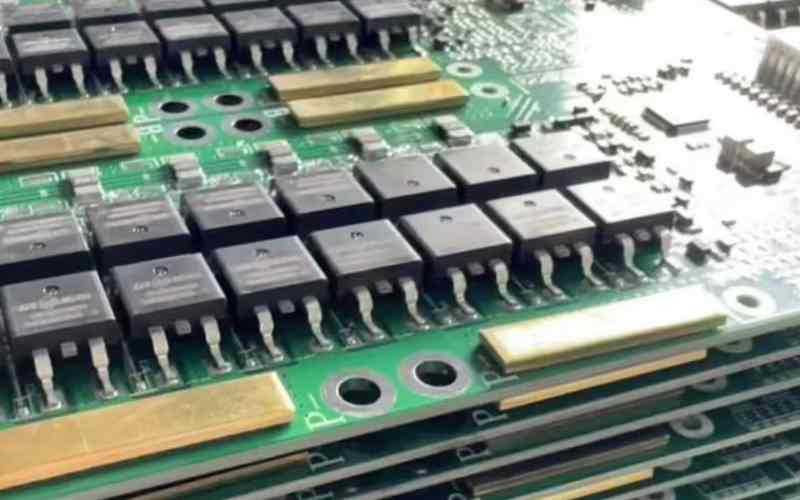
Innovative Breakthroughs in PCB Manufacturing and Assembly Services
Innovative Breakthroughs in PCB Manufacturing and Assembly Services
In the ever - evolving landscape of electronics, Printed Circuit Boards (PCBs) serve as the fundamental building blocks that enable the functionality of a vast array of devices, from smartphones and laptops to industrial automation systems and medical equipment. As technology advances at an unprecedented pace, the demand for more sophisticated, high - performance, and reliable PCBs has surged. This has spurred continuous innovation in PCB manufacturing and assembly services, and ShwayPCB stands at the forefront of these groundbreaking developments.
The Evolution of PCB Manufacturing and Assembly
Historical Perspective
The history of PCBs dates back to the early 20th century, with the first simple PCBs being used in radio equipment. Initially, PCBs were relatively basic, consisting of single - layer boards with through - hole components. Over time, as the need for more complex and compact electronic devices grew, multi - layer PCBs were introduced, allowing for increased component density and improved electrical performance.
The development of Surface Mount Technology (SMT) in the 1960s and 1970s was a major milestone in PCB assembly. SMT enabled components to be mounted directly onto the surface of the PCB, eliminating the need for through - holes and significantly reducing the size of the final product. This innovation paved the way for the miniaturization of electronic devices that we see today.
Current Market Trends
In the current market, the global PCB industry is experiencing robust growth. According to market research reports, the global PCB market size was valued at approximately 80 billion by 2027, growing at a CAGR of around 6% during the forecast period. This growth is driven by several factors, including the increasing adoption of IoT devices, the rise of 5G technology, and the growing demand for electric vehicles.
The following table illustrates the projected growth of the PCB market by application segment from 2022 to 2027:
| Application Segment | 2022 Market Size ($ billion) | 2027 Projected Market Size ($ billion) | CAGR (%) |
|---|---|---|---|
| Consumer Electronics | 20 | 26 | 5.5 |
| Automotive | 10 | 15 | 8.5 |
| Industrial | 12 | 16 | 6.0 |
| Medical | 5 | 7 | 7.0 |
| Others | 13 | 17 | 5.5 |
Innovative Breakthroughs in PCB Manufacturing
Advanced Material Technologies
One of the key areas of innovation in PCB manufacturing is the development of advanced materials. Traditional FR4 materials, while widely used, have limitations in terms of high - frequency performance and thermal management. To address these challenges, new materials such as high - frequency laminates (e.g., Rogers materials) and metal - core PCBs are gaining popularity.
High - frequency laminates offer excellent electrical properties, including low dielectric constant and low loss tangent, making them ideal for applications in 5G communication, radar systems, and high - speed data transmission. Metal - core PCBs, on the other hand, provide superior thermal conductivity, allowing for efficient heat dissipation in high - power applications such as LED lighting and power electronics.
The table below compares the key properties of traditional FR4 and high - frequency laminates:
| Property | FR4 | High - Frequency Laminate (e.g., Rogers 4350B) |
|---|---|---|
| Dielectric Constant (Dk) | 4.2 - 4.8 | 3.48 - 3.66 |
| Loss Tangent (Df) | 0.015 - 0.025 | 0.002 - 0.004 |
| Thermal Conductivity (W/m·K) | 0.2 - 0.3 | 0.3 - 0.5 |
| Glass Transition Temperature (Tg, °C) | 130 - 180 | 280 - 300 |
High - Precision Manufacturing Processes
Another significant breakthrough in PCB manufacturing is the advancement of high - precision manufacturing processes. With the increasing demand for miniaturization and high - density interconnects, PCB manufacturers are investing in state - of - the - art equipment and technologies to achieve tighter tolerances and higher component densities.
Laser drilling technology has revolutionized the production of microvias in PCBs. Microvias are small holes that connect different layers of a multi - layer PCB, enabling higher component density and improved signal integrity. Laser drilling can create microvias with diameters as small as 25 microns, which is much smaller than what can be achieved with traditional mechanical drilling methods.
In addition, advanced imaging and inspection systems are being used to ensure the quality and accuracy of PCB manufacturing. Automated Optical Inspection (AOI) and X - ray inspection systems can detect defects such as misaligned components, solder voids, and internal layer shorts with high precision, reducing the risk of defective products reaching the market.
Innovative Breakthroughs in PCB Assembly
High - Precision Mixed - Technology Assembly
PCB Assembly has also witnessed significant innovations, particularly in the area of high - precision mixed - technology assembly. Mixed - technology assembly combines SMT and Through - Hole Technology (THT) to take advantage of the benefits of both methods. SMT is used for small, surface - mount components, while THT is used for larger, through - hole components that require higher mechanical strength.
Advanced pick - and - place machines are capable of handling components with extremely small pitches, as low as 0.2mm. These machines use high - precision vision systems to accurately place components on the PCB, ensuring reliable soldering and high - quality assembly. In addition, the use of lead - free soldering materials and processes has become standard in the industry, in compliance with environmental regulations such as RoHS.
The following table compares the key features of SMT and THT assembly:
| Feature | SMT Assembly | THT Assembly |
|---|---|---|
| Component Size | Small (e.g., 0201, 0402 resistors) | Large (e.g., connectors, switches) |
| Component Placement Speed | High (up to 50,000 components per hour) | Lower (up to 5,000 components per hour) |
| Soldering Method | Reflow soldering | Wave soldering or manual soldering |
| Mechanical Strength | Lower | Higher |
| Component Density | High | Lower |
Automation and Industry 4.0 Integration
Automation and Industry 4.0 technologies are transforming the PCB assembly process. Automated assembly lines are being implemented to improve efficiency, reduce labor costs, and enhance product quality. These assembly lines are equipped with robots that can perform tasks such as component picking, placement, and soldering with high precision and consistency.
Industry 4.0 technologies, such as the Internet of Things (IoT) and big data analytics, are being used to monitor and optimize the PCB assembly process in real - time. Sensors are installed on the assembly equipment to collect data on parameters such as temperature, humidity, and component placement accuracy. This data is then analyzed using big data analytics tools to identify potential issues and optimize the assembly process for improved efficiency and quality.
ShwayPCB: Leading the Way in Innovative PCB Manufacturing and Assembly
Comprehensive PCB Manufacturing and Assembly Services
ShwayPCB is a leading provider of PCB manufacturing and assembly services, offering a comprehensive range of solutions to meet the diverse needs of customers across various industries. The company's manufacturing capabilities include single - layer, double - layer, and multi - layer PCBs, as well as flexible and rigid - flex PCBs. It can handle a wide range of materials, including traditional FR4, high - frequency laminates, and metal - core substrates.
In terms of PCB assembly, ShwayPCB specializes in high - precision mixed - technology assembly, combining SMT and THT to deliver reliable and high - quality products. The company's assembly lines are equipped with advanced pick - and - place machines, reflow ovens, and wave soldering equipment to ensure efficient and accurate assembly.
Turnkey PCB Assembly Solutions
For customers looking for a hassle - free and end - to - end solution, ShwayPCB offers Turnkey PCB Assembly services. This comprehensive service covers everything from PCB design review, component procurement, PCB manufacturing, and assembly to testing and packaging. By choosing the turnkey solution, customers can save time and resources, as ShwayPCB manages the entire process on their behalf, ensuring seamless coordination and timely delivery.
The turnkey PCB assembly process at ShwayPCB involves the following steps:
- Design Review: The company's team of experienced engineers carefully reviews the customer's PCB design files to identify any potential issues or areas for improvement. They provide detailed feedback and suggestions to optimize the design for manufacturability and cost - effectiveness.
- Component Procurement: ShwayPCB leverages its extensive network of trusted suppliers to source high - quality components at competitive prices. The procurement team ensures that all components meet the required specifications and are delivered on time to avoid production delays.
- PCB Manufacturing: Using advanced manufacturing equipment and processes, the company produces high - precision PCBs that meet the customer's exact requirements. The quality control team performs rigorous inspections at every stage of the manufacturing process to ensure that the PCBs are free from defects.
- PCB Assembly: Skilled technicians assemble the PCBs using the appropriate SMT and THT techniques, depending on the component types and design complexity. High - quality soldering materials and industry - standard assembly procedures are followed to ensure reliable and long - lasting connections.
- Testing and Quality Control: Comprehensive testing is conducted on the assembled PCBs to verify their functionality and performance. Testing methods include in - circuit testing (ICT), functional testing, and X - ray inspection to detect any hidden defects.
- Packaging and Delivery: Once the PCBs pass all quality checks, they are carefully packaged to protect them during transportation. The company arranges for timely delivery to the customer's specified location, ensuring that the products are received in perfect condition.
Quick Turn PCB Assembly Services
In today's fast - paced business environment, time - to - market is a critical factor in the success of any electronic product. To help customers meet their tight deadlines, ShwayPCB offers Quick Turn PCB Assembly services. The company maintains a large inventory of commonly used components and has dedicated production lines for fast - track projects. Its streamlined processes and efficient supply chain management enable it to quickly respond to urgent requirements and deliver high - quality PCBs in as little as 24 hours.
The Future of PCB Manufacturing and Assembly
Looking ahead, the future of PCB manufacturing and assembly is likely to be shaped by several key trends. The continued miniaturization of electronic devices will drive the demand for even smaller and more complex PCBs, requiring further advancements in manufacturing and assembly technologies. The integration of artificial intelligence (AI) and machine learning (ML) in the PCB manufacturing and assembly process is expected to improve efficiency, quality, and cost - effectiveness.
In addition, the development of new materials and packaging technologies, such as 3D - printed PCBs and system - in - package (SiP) solutions, will open up new possibilities for electronic device design and functionality. As the electronics industry continues to evolve, ShwayPCB remains committed to staying at the forefront of innovation, providing customers with cutting - edge PCB manufacturing and assembly services.
Contact Us Today
If you are looking for innovative and reliable PCB manufacturing and assembly services, look no further than ShwayPCB. With its state - of - the - art facilities, experienced team, and commitment to quality, the company is well - equipped to meet your most demanding requirements. Contact us today at yuan@shwaypcb.com or visit our website at https://fr4pcb.tech/ to learn more about our services and request a quote.
In conclusion, the field of PCB manufacturing and assembly is experiencing a period of rapid innovation, driven by the increasing demand for high - performance and reliable electronic devices. ShwayPCB is at the forefront of these developments, offering a comprehensive range of innovative services that enable customers to bring their electronic products to market faster and more efficiently.