We use cookles to Improve your online experience. By continuing browsing this website, we assume you agree our use of cookies.

How HDI PCB Manufacturing Differs from Standard PCB Manufacturing
September 2nd, 2025
365 views
How HDI PCB Manufacturing Differs from Standard PCB Manufacturing
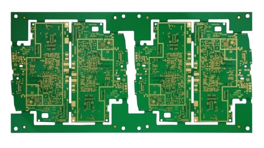
High-Density Interconnect (HDI) PCB manufacturing and standard PCB manufacturing are distinct in nearly every technical stage—from the materials used to the equipment deployed. Standard PCB manufacturing relies on decades-old, cost-optimized processes designed for larger traces, through-holes, and low-complexity devices (e.g., remote controls, power supplies). In contrast, HDI PCB Manufacturing employs advanced techniques to produce microvias, fine-pitch component-compatible layouts, and high-layer boards—critical for 5G smartphones, medical wearables, and automotive ADAS modules. These differences directly translate to HDI’s core advantages: miniaturization, high-frequency performance, and density.
To fully grasp why HDI PCBs outperform standard PCBs in advanced applications, it’s essential to examine how each manufacturing stage differs. This guide provides a technical, side-by-side comparison, with insights from ShwayPCB—a leader in PCB manufacturing process and board types.
1. Stage 1: Material Selection & Preparation
The foundation of any PCB lies in its materials, and HDI manufacturing demands substrates and components that can support ultra-fine features—unlike standard PCB manufacturing, which uses lower-cost, less specialized materials.
|
Aspect
|
Standard PCB Manufacturing
|
HDI PCB Manufacturing
|
|
Substrate Type
|
Standard FR4 (Tg=130–150°C); thick copper (1–2oz)
|
High-Tg FR4 (Tg=170–180°C), polyimide (for flexible HDI PCB), or low-loss substrates (Rogers 4350B for RF HDI PCB); ultra-thin copper (0.5–1oz)
|
|
Component Compatibility
|
Through-hole components, 0402+ passives, ≥0.5mm-pitch BGAs
|
SMT-only: 01005 passives, 0.3mm-pitch BGAs/CSPs, fine-pitch microchips
|
|
Prepreg (Adhesive)
|
Standard FR4 prepreg (thickness ≥0.1mm)
|
Ultra-thin prepreg (0.05–0.08mm); adhesive-less bonding for flexible HDI
|
Key Rationale for Differences
- Substrate Tg: Standard PCBs use low-Tg FR4 because they operate at mild temperatures and do not require tight dimensional stability. HDI PCBs need high-Tg substrates to withstand laser drilling heat (up to 300°C) and prevent warpage during sequential lamination. For example, ShwayPCB uses Tg=180°C FR4 for automotive HDI PCBs, ensuring stability under hood temperatures (-40°C to +125°C).
- Component Size: Standard PCBs accommodate larger components because mechanical drilling limits via density. HDI’s microvias enable ultra-small SMT components, reducing board size by 40–60%. A standard PCB for an IoT sensor (50mm × 50mm) shrinks to 25mm × 25mm with HDI.
- Prepreg Thickness: Standard PCBs use thick prepreg to simplify mass lamination. HDI requires thin prepreg to maintain thin profiles (≤0.4mm) and ensure reliable microvia plating—critical for wearables and medical devices.
2. Stage 2: Drilling (The Defining HDI Process)
Drilling is the most significant point of divergence. Standard PCBs use mechanical drills for large through-holes, while HDI PCBs rely on laser drilling to create microvias—enabling high density.
|
Aspect
|
Standard PCB Manufacturing
|
HDI PCB Manufacturing
|
|
Equipment
|
Mechanical drills (tungsten carbide bits)
|
UV/CO₂ lasers; femtosecond lasers for ultra-HDI (≤0.05mm microvias)
|
|
Via Size Range
|
≥0.3mm (12mil) through-holes; limited blind vias (≥0.5mm)
|
≤0.15mm (6mil) microvias; blind/buried vias down to 0.1mm (4mil)
|
|
Placement Accuracy
|
±0.03mm (drill wander common)
|
±0.005mm (UV lasers); ±0.002mm (femtosecond lasers)
|
|
Throughput
|
500–1,000 vias/min (large holes)
|
2,000–5,000 microvias/min (UV lasers); lower for ultra-small vias
|
Key Rationale for Differences
- Mechanical vs. Laser Drilling: Mechanical drills cannot create holes smaller than 0.3mm—attempting to do so causes bit breakage and trace damage. Laser drilling vaporizes material without contact, enabling microvias. ShwayPCB uses UV lasers for 0.1mm microvias, ensuring no heat damage to surrounding traces.
- Through-Holes vs. Microvias: Standard through-holes span all layers, wasting 20–30% of board space. HDI microvias connect only 1–2 layers, freeing space for components. A 50mm × 50mm HDI PCB fits 200+ components vs. 80–100 on a standard PCB of the same size.
- Accuracy Needs: Fine-pitch components (0.3mm BGAs) require microvias aligned to ±0.005mm—mechanical drills cannot meet this tolerance. Laser drilling’s precision reduces rework by 80% vs. standard PCBs.
3. Stage 3: Lamination (Building Multi-Layer Boards)
Lamination differs drastically: standard PCBs use "mass lamination" for simplicity, while HDI uses sequential lamination to enable high-layer counts and precise alignment.
|
Aspect
|
Standard PCB Manufacturing
|
HDI PCB Manufacturing
|
|
Technique
|
Mass lamination (all layers pressed at once)
|
Sequential lamination (layers added one at a time; drilled/plated between steps)
|
|
Alignment Method
|
Pin alignment (±0.05mm tolerance)
|
Automated Optical Alignment (AOA) (±0.01mm tolerance)
|
|
Max Layer Count
|
12 layers (alignment errors compound with layers)
|
24–40 layers (sequential stacking avoids errors)
|
|
Cycle Time
|
1–2 hours (entire stack); no intermediate steps
|
3–4 hours/layer (drilling + plating + lamination); 12–16 hours for 4 layers
|
Key Rationale for Differences
- Mass vs. Sequential Lamination: Standard mass lamination is fast but causes layer shifting (±0.05mm), making blind/buried vias unreliable. HDI’s sequential process adds one layer at a time, using AOA (5MP cameras) to align each new layer. ShwayPCB’s AOA ensures ±0.01mm precision—critical for 8-layer RF HDI PCB designs, where misaligned vias cause signal loss.
- Layer Count Limits: Standard PCBs max out at 12 layers because alignment errors worsen with each layer. HDI’s sequential process enables 40-layer boards for aerospace applications (e.g., satellite modules).
- Intermediate Processing: Standard lamination has no mid-process steps—all drilling/plating happens before stacking. HDI drills and plates microvias between layers, ensuring 99.5% interconnect reliability vs. 97% for standard PCBs.
4. Stage 4: Plating (Ensuring Conductive Paths)
Plating is critical for via and trace conductivity. HDI manufacturing requires precision plating to coat microvias uniformly, while standard PCBs use simpler methods for larger through-holes.
|
Aspect
|
Standard PCB Manufacturing
|
HDI PCB Manufacturing
|
|
Technique
|
Electroless copper (2–3μm) + DC electrolytic copper (18–22μm)
|
Electroless nickel-boron (ENB, 2–3μm) + pulse electrolytic copper (20–35μm)
|
|
Microvia Coverage
|
Inconsistent; voids common (>5% of vias)
|
Uniform coverage; voids <1% (per IPC-6012)
|
|
Trace Tolerance
|
±10% (thickness variation)
|
±5% (critical for controlled impedance)
|
|
Surface Finish
|
Hot air solder leveling (HASL); limited ENIG
|
ENIG (standard for fine-pitch); immersion silver for cost-sensitive HDI
|
Key Rationale for Differences
- ENB vs. Electroless Copper: Standard electroless copper has poor step coverage, leaving microvias with voids. HDI uses ENB plating, which adheres better to laser-drilled walls and ensures 99% void-free microvias (vs. 70% for standard copper).
- Pulse Plating: Standard DC plating causes "dog boning" (thicker plating at via openings), narrowing microvias. HDI’s pulse plating (alternating current) deposits copper evenly, maintaining ±5% trace tolerance—essential for RF HDI PCB impedance control (50Ω ±5%).
- Surface Finishes: HASL leaves uneven solder deposits, making it unsuitable for 0.3mm-pitch BGAs. HDI uses ENIG, a flat, uniform finish that ensures reliable solder joints. ShwayPCB’s ENIG meets IPC-4522 standards (nickel: 5μm ±10%, gold: 0.1μm ±10%).
5. Stage 5: Etching (Creating Trace Patterns)
Etching removes excess copper to form traces. HDI manufacturing uses precise methods to maintain fine trace widths, while standard etching tolerates wider variations.
|
Aspect
|
Standard PCB Manufacturing
|
HDI PCB Manufacturing
|
|
Method
|
Spray etching (ferric/cupric chloride)
|
Plasma etching (ultra-fine traces) + spray etching
|
|
Trace Width Tolerance
|
±0.02mm (for 0.127mm traces)
|
±0.005mm (for 0.0762mm traces)
|
|
Undercut Control
|
High undercut (0.01–0.015mm); weakens fine traces
|
Low undercut (≤0.005mm); maintains trace integrity
|
|
Mask Alignment
|
Photoresist (±0.02mm shift)
|
Laser Direct Imaging (LDI) (±0.002mm)
|
Key Rationale for Differences
- Plasma vs. Spray Etching: Standard spray etching is aggressive, causing undercut that weakens fine traces. HDI uses plasma etching for ≤0.0762mm traces, reducing undercut by 70% and ensuring ±0.005mm tolerance—critical for high-frequency signal integrity.
- LDI vs. Photoresist: Standard photoresist alignment relies on masks that shift (±0.02mm). HDI’s LDI (direct laser writing) achieves ±0.002mm alignment, reducing short circuits by 90% vs. standard masking.
6. Stage 6: Inspection & Testing (Ensuring Quality)
HDI PCBs require far more rigorous testing to catch defects in fine features—standard methods like 2D AOI are insufficient.
|
Aspect
|
Standard PCB Manufacturing
|
HDI PCB Manufacturing
|
|
Visual Inspection
|
2D AOI (surface defects only); manual through-hole checks
|
3D AOI (trace height/width); 3D X-ray (microvia plating)
|
|
Electrical Testing
|
Continuity (open/short); basic impedance checks
|
TDR (impedance ±5%); flying probe (fine-pitch components)
|
|
Reliability Testing
|
Thermal cycling (500 cycles); no vibration testing
|
Thermal cycling (1,000–5,000 cycles); vibration (MIL-STD-883H)
|
|
Yield Target
|
97–98% (acceptable for low-complexity)
|
99.2–99.5% (required for high-cost HDI)
|
Key Rationale for Differences
- 3D X-ray for Microvias: Standard 2D AOI cannot see inside microvias, missing voids or incomplete plating. HDI’s 3D X-ray inspects via walls, detecting 5μm voids—preventing field failures in medical devices. ShwayPCB uses 3D X-ray for 100% of HDI orders.
- TDR Impedance Testing: Standard PCBs only check for opens/shorts, but HDI’s high-frequency applications need precise impedance. TDR measures impedance along each trace, flagging deviations >5%.
- Reliability Testing: Standard PCBs undergo minimal testing because their low complexity reduces risk. HDI PCBs (used in ADAS/medical devices) undergo 1,000+ thermal cycles and vibration testing—ensuring <0.1% field failure rates.
7. FAQ: HDI vs. Standard PCB Manufacturing
1. Why is HDI PCB manufacturing more expensive?
HDI costs more due to:
- Specialized Equipment: Laser drills (\(500k–\)1M) and 3D X-ray systems (\(300k–\)500k) are far costlier than standard mechanical drills (\(50k–\)100k) and 2D AOI (\(100k–\)200k).
- Slower Throughput: Sequential lamination and laser drilling take 2–3x longer than standard processes.
- Higher Materials: High-Tg FR4 and Rogers substrates cost 20–30% more than standard FR4.
However, HDI’s smaller size and lower failure rates reduce total cost of ownership (TCO) by 25–30% for complex designs—ShwayPCB clients recoup upfront costs within 6 months.
2. Can standard PCB manufacturers upgrade to produce HDI?
Yes, but it requires significant investment:
- Equipment: Adding UV lasers, sequential lamination presses, 3D X-ray, and LDI (\(1.5M–\)3M total).
- Training: Engineers need 6–12 months to master laser drilling, ENB plating, and sequential lamination.
- Quality Overhaul: Implementing 100% X-ray inspection and microvia traceability.
Most manufacturers find partnering with HDI specialists like ShwayPCB more cost-effective.
3. How do lead times compare?
HDI has longer lead times due to complexity:
- Prototypes: 5–7 days (HDI) vs. 3–5 days (standard).
- Low-Volume (1k units): 10–14 days (HDI) vs. 7–10 days (standard).
- High-Volume (100k units): 2–3 weeks (HDI) vs. 1–2 weeks (standard).
ShwayPCB offers expedited HDI prototyping (3–4 days) for time-critical projects.
4. Is HDI manufacturing compatible with standard SMT assembly?
Yes, but HDI requires high-precision SMT machines (±0.015mm accuracy) to place 0.3mm-pitch BGAs. Standard SMT machines (±0.03mm) may struggle with fine-pitch components. ShwayPCB’s SMT lines (Yamaha YSM40R) handle HDI’s fine-pitch components with 99.8% placement accuracy.
5. What happens if HDI manufacturing defects occur?
HDI defects (e.g., microvia voids) are harder to repair than standard PCB defects, but ShwayPCB uses:
- Laser Ablation: Removes damaged microvia plating for rework.
- Micro-Soldering: Repairs 0.3mm-pitch BGAs with 5μm-tip precision.
Repair success rates are 80–90% for HDI, vs. 95% for standard PCBs—emphasizing the need for rigorous HDI quality control.
8. Conclusion
HDI PCB manufacturing differs from standard PCB manufacturing in every technical stage—from laser drilling microvias to sequential lamination and 3D X-ray testing. These differences enable HDI’s unique advantages: miniaturization, high-frequency performance, and reliability—traits that have become non-negotiable for next-generation electronics. Standard PCB manufacturing, while cost-effective for low-complexity devices (e.g., remote controls, basic sensors), cannot meet the demands of 5G modems, medical implants, or automotive ADAS systems—applications where even a 0.1mm reduction in board size or 1dB reduction in signal loss can define product success.
At the heart of HDI’s superiority lies its ability to turn design constraints into opportunities: ultra-fine traces and microvias transform bulky multi-board assemblies into single, compact HDI PCBs; sequential lamination enables 40-layer designs that integrate power, signal, and RF functions; and precision plating ensures <1% microvia voids, critical for mission-critical medical or aerospace devices. These advancements are not just technical feats—they translate to tangible business value: reduced enclosure costs (30–50%), lower field failure rates (<0.1% for medical HDI), and faster time-to-market (via quickturn HDI PCB prototyping).
ShwayPCB’s expertise in PCB manufacturing process and board types positions it as a trusted partner for bridging the gap between HDI design and production. Our specialized equipment—UV lasers for 0.1mm microvias, 3D X-ray systems for plating inspection, and AOA for sequential lamination—ensures 99.5% first-pass yield for HDI PCBs, exceeding industry averages of 97–98%. Whether you’re developing a flexible HDI PCB for a wearable ECG monitor, an RF HDI PCB for 5G radar, or a high-layer HDI for satellite communication, our team provides end-to-end support: from DFM optimization (to avoid common HDI pitfalls like undersized microvias) to post-production documentation (for regulatory compliance like ISO 13485 or IATF 16949).
The choice between HDI and standard PCB manufacturing ultimately hinges on your application’s requirements. If your product demands miniaturization, high-frequency performance, or fine-pitch component integration, HDI is not just a "better" option—it is the only viable one. Standard PCBs will remain a staple for low-complexity projects, but as electronics grow smaller, smarter, and more connected, HDI PCB manufacturing will continue to be the backbone of innovation.
To discuss your HDI PCB project, request a technical consultation, or get a customized quote for HDI PCB Manufacturing, contact ShwayPCB at yuan@shwaypcb.com. For detailed specifications on our HDI capabilities—including material options (Rogers 4350B, polyimide), layer counts (2–40 layers), and testing protocols (TDR, thermal cycling)—visit our dedicated PCB manufacturing page.

Copyright © 2005-2025 ShwayPCB : PCB Fabrication and Assembly Manufacturer. All Rights Reserved. POWERED BY UEESHOP


Copyright © 2005-2025 ShwayPCB : PCB Fabrication and Assembly Manufacturer. All Rights Reserved. POWERED BY UEESHOP