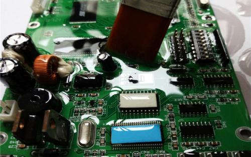
High-Precision PCB Assembly: Mastering HDI, BGA, and Flex Circuits with Turnkey Solutions
High-Precision PCB Assembly: Mastering HDI, BGA, and Flex Circuits with Turnkey Solutions
Introduction: Technological Evolution and Market Demands in High-Precision PCB Assembly
Driven by emerging technologies such as 5G communication, artificial intelligence (AI), and the Internet of Things (IoT), electronic devices are evolving towards miniaturization, high performance, and multifunctionality at an accelerated pace. This trend imposes stringent requirements on printed circuit board (PCB) manufacturing and assembly: wiring density must surpass traditional limits, signal transmission speeds must reach the GHz level, while simultaneously addressing thermal management, electromagnetic compatibility (EMC), and long-term reliability. As the global hub for PCB manufacturing, China has established a comprehensive industrial ecosystem covering design, materials, processes, and testing. Among these advancements, high-precision PCB assembly (PCB Assembly) technologies—particularly the integration of High-Density Interconnect (HDI), Ball Grid Array (BGA) packaging, and flexible circuits (Flex Circuits)—are emerging as key drivers of industry transformation.
This article systematically analyzes the core technologies of high-precision PCB assembly from four dimensions: technical principles, manufacturing challenges, solutions, and industry practices. It also explores how Turnkey (one-stop) solutions facilitate seamless integration from design to mass production.
I. Core Technologies of High-Precision PCB Assembly
1. HDI Technology: The Microvia Revolution Breaking Spatial Limits
HDI (High-Density Interconnector) achieves exponential increases in wiring density within limited areas through laser drilling, blind/buried vias, and build-up processes. Its key technical advantages include:
- Microvia diameters ≤0.1mm: Laser drilling achieves ±5μm precision, an 80% improvement over traditional mechanical drilling, significantly saving routing space. For example, smartphone motherboards adopting HDI technology can compress 12 traditional layers into 8, reducing area by 40%.
- Blind/buried via structures: Blind vias connect outer and inner layers, while buried vias connect inner layers, eliminating full-through vias that occupy signal layers and reducing crosstalk risks. A server motherboard case study demonstrated that blind/buried via designs improved eye diagram opening by 15% for high-speed signals (e.g., PCIe 5.0), reducing bit error rates to below 10⁻¹².
- Fine-line manufacturing: Line widths/spacing (L/S) as low as 3mil (75μm), combined with high-purity low-roughness copper foil, reduce DC resistance by 20% and signal attenuation by 3dB/m (at 10GHz).
Manufacturing Challenges: Laser drilling requires balancing energy density and heat-affected zones (HAZ) to prevent substrate carbonization. Electroless copper plating for via filling must control uniformity to avoid voids that compromise reliability.
2. BGA Packaging: Reliable Interconnection for High Pin Density
BGA achieves electrical connections between chips and PCBs through array-based solder balls, offering advantages such as:
- Increased pin density: A 0.4mm pitch BGA package can integrate 1,000+ pins, a 5x improvement over Quad Flat Package (QFP) designs, meeting the high I/O demands of high-performance processors (e.g., FPGAs, ASICs).
- Shortened signal paths: Direct solder ball contact with PCB pads reduces parasitic inductance by 80% compared to wire-bonded packages, significantly optimizing signal integrity (SI). Testing shows BGA-packaged DDR5 memory modules achieve 30% higher timing margins at 3200MT/s compared to TSOP packages.
- Enhanced thermal performance: Bottom thermal pads rapidly dissipate chip heat, while thermal vias reduce junction-to-ambient thermal resistance (RθJA) to below 10°C/W.
Manufacturing Challenges: BGA solder joints are invisible, requiring X-ray inspection and automated optical inspection (AOI) to ensure quality. Solder ball coplanarity must be controlled within ±0.05mm to prevent voids or shorts.
3. Flexible Circuits (Flex Circuits): Three-Dimensional Freedom in Interconnection
Flexible circuits use polyimide (PI) or polyester (PET) substrates to enable three-dimensional interconnects through dynamic (repeated bending) or static (fixed bending) applications. Key characteristics include:
- Controllable bending radii: Single-layer flex circuits achieve minimum bending radii of 0.1mm, meeting compact design requirements for wearables (e.g., smartwatches).
- High-density routing: Combined with HDI technology, flex circuits achieve 4mil L/S and integrate rigid-flex structures, replacing traditional cables to reduce assembly steps and failure points.
- Environmental durability: PI substrates withstand glass transition temperatures (Tg) up to 350°C and operate reliably between -55°C and 125°C, suitable for automotive and aerospace applications.
Manufacturing Challenges: Flexible substrates exhibit lower dimensional stability than FR-4, requiring tension control and compensation designs to minimize layer misalignment. Coverlay lamination must avoid bubbles to prevent moisture ingress and insulation failure.
II. Turnkey PCB Assembly: The Value of One-Stop Solutions
1. End-to-End Process Control from Design to Mass Production
Turnkey models integrate PCB design, manufacturing, assembly, and testing to provide "hands-off" services, with advantages including:
- Design for Manufacturability (DFM) optimization: During PCB design, engineers use EDA tools (e.g., Cadence Allegro) for 3D modeling and interference checks to preempt manufacturing risks. For example, DFM analysis helped a medical device client adjust BGA pad dimensions from 0.3mm to 0.35mm, improving soldering yield from 85% to 98%.
- Supply chain collaboration: Turnkey suppliers partner with material manufacturers (e.g., Shengyi Technology, Taiyo Ink) to ensure stable supply of high-frequency materials (e.g., Rogers 4350B) and high-Tg laminates (e.g., IT180A), reducing lead times to 72 hours (Quick Turn services).
- Automated assembly lines: Siemens SIPLACE pick-and-place machines and ERSA reflow ovens enable 01005 (0.4mm×0.2mm) component placement with ±0.03mm precision and single-line capacity of 300,000 points/day.
2. Industry-Leading Quality Control Systems
High-precision PCB assembly requires multi-level testing for reliability:
- Electrical testing (ICT/FCT): Flying probe testers (e.g., Spea 3030) achieve 100% open/short coverage, while functional testing (FCT) simulates real-world scenarios to validate power, clock, and communication modules.
- Reliability testing: Highly Accelerated Life Testing (HALT), Highly Accelerated Stress Screening (HASS), and temperature cycling (-40°C to 125°C, 1,000 cycles) ensure compliance with IPC-6012 Class 3 standards.
- Failure analysis (FA): Scanning electron microscopy (SEM) and energy-dispersive spectroscopy (EDS) identify root causes of soldering defects. For instance, FA resolved a BGA open-circuit issue by adjusting stencil thickness and printing pressure, reducing defect rates from 0.5% to 0.02%.
III. Industry Practices: Technological Breakthroughs by Chinese PCB Manufacturers
1. HDI+BGA+Flex Integration by a Guangdong Enterprise
This company provided motherboard assembly for an international smartwatch brand, integrating 10-layer HDI with rigid-flex design and BGA-packaged processors. Key achievements include:
- Stacked blind/buried vias: Three-stage blind vias (0.1mm diameter) connected processors to memory modules, reducing signal propagation delay to 200ps—a 40% improvement over traditional designs.
- Dynamic flex bending: PI substrates with reinforced copper foil withstood 100,000 bending cycles (2mm radius) without fracture, meeting consumer-grade durability requirements.
- Hybrid material press: High-frequency signal layers used PTFE (Dk=2.2) while other layers used FR-4, balancing cost and performance to achieve ≤0.5dB/100mm insertion loss at 5G frequencies (24-40GHz).
2. Quick Turn Services by an East China Enterprise
This company delivered 48-hour prototyping for a startup by:
- Digital factory deployment: MES (Manufacturing Execution System) and APS (Advanced Planning and Scheduling) enabled end-to-end visibility, reducing manual intervention and wait times.
- Modular design library: A library of 2,000+ standard modules (e.g., power management, sensor interfaces) allowed clients to reuse designs, cutting development time from 7 days to 2.
- Concurrent engineering: Component procurement and SMT programming ran in parallel with PCB manufacturing, reducing assembly preparation time by 60%.
Conclusion: The Future of High-Precision PCB Assembly
As AI computing demands explode and 6G technology nears commercialization, PCB assembly will evolve toward higher density, speed, and reliability. Turnkey models are reshaping the industry ecosystem: leading firms build cost barriers through vertical integration (e.g., in-house material plants), while smaller players pursue differentiation via specialization (e.g., flexible circuits or high-frequency materials). For clients, selecting Turnkey suppliers with full HDI, BGA, and Flex capabilities has become critical for shortening R&D cycles, mitigating project risks, and enhancing product competitiveness.
Contact Email: yuan@shwaypcb.com
Website: https://fr4pcb.tech/