We use cookles to Improve your online experience. By continuing browsing this website, we assume you agree our use of cookies.

Home > Blog > PCB technology > High Density Interconnect PCB: Precision Solutions from Trusted HDI PCB Manufacturer
High Density Interconnect PCB: Precision Solutions from Trusted HDI PCB Manufacturer
September 16th, 2025
205 views
High Density Interconnect PCB: Precision Solutions from Trusted HDI PCB Manufacturer
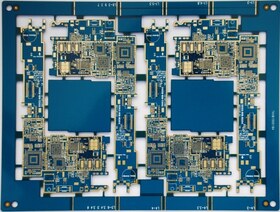
In the era of miniaturized electronics—from 5G modules and wearable devices to automotive ADAS (Advanced Driver Assistance Systems)—the demand for PCBs that deliver higher component density, faster signal transmission, and smaller form factors has never been greater. High Density Interconnect (HDI) PCBs address this need by leveraging microvia technology, dense copper routing, and thin-core substrates to pack more functionality into limited space. As a leading HDI PCB manufacturer, ShwayPCB specializes in producing high-performance high density interconnect PCBs tailored to industries like IoT, automotive, and medical electronics. This article explores the technical advantages of high density interconnect PCBs, the capabilities of a top-tier microvia HDI PCB manufacturer, application-specific solutions, quality control protocols, and answers critical procurement questions—providing a comprehensive guide for engineers and buyers seeking reliable HDI solutions.
1. Technical Advantages of High Density Interconnect PCBs
High density interconnect PCBs outperform traditional PCBs in key areas, making them indispensable for modern compact electronics. A reputable HDI PCB manufacturer leverages these advantages to meet strict design requirements:
- Microvia Technology: The defining feature of HDI PCBs, microvias (diameter ≤ 0.15mm, aspect ratio 1:1) enable vertical interconnection between layers without occupying excessive board space. Unlike traditional through-hole vias (which can block 30–40% of surface area), microvias free up 60% more space for components—critical for devices like smartwatches (with PCBs as small as 15mm × 20mm) and 5G mmWave modules.
- Higher Routing Density: High density interconnect PCBs support trace widths/spacings as tight as 2mil/2mil (0.05mm/0.05mm), compared to 3mil/3mil for standard PCBs. This increases routing density by 50%, allowing integration of complex circuits (e.g., multi-core processors, high-speed transceivers) in miniaturized enclosures.
- Improved Signal Integrity: The short, direct paths of microvias reduce signal skew and crosstalk—critical for high-frequency applications (up to 40GHz for 5G). A qualified HDI PCB manufacturer optimizes trace impedance (50Ω ±10% for RF signals) and uses low-loss substrates (Df ≤ 0.004 at 10GHz) to ensure stable signal transmission.
- Thinner Profile: High density interconnect PCBs use thin-core substrates (0.1mm–0.2mm per layer) and reduced copper thickness (0.5oz–1oz), resulting in overall board thickness as low as 0.3mm—ideal for wearable devices (e.g., fitness trackers) and slim consumer electronics (e.g., foldable phones).
2. Capabilities of a Leading HDI PCB Manufacturer
To fully leverage the benefits of high density interconnect PCBs, partnering with a capable HDI PCB manufacturer is essential. ShwayPCB, as a specialized microvia HDI PCB manufacturer and 2-12 layer HDI PCB manufacturer, offers technical capabilities that meet global industry standards:
- Layer Count & Microvia Configurations: Supports 2–12 layer HDI PCBs with sequential lamination (build-up) and various microvia types:
- Blind vias (connect outer layers to inner layers).
- Buried vias (connect inner layers only).
- Stacked vias (multiple microvias stacked vertically for multi-layer interconnection).
For example, a 6-layer HDI PCB for an IoT sensor uses stacked microvias to connect a Bluetooth chip (outer layer) to a power management IC (inner layer), reducing board size by 40% compared to a traditional 6-layer PCB.
- Precision Manufacturing Equipment: Utilizes advanced machinery to ensure microvia accuracy:
- Laser drilling machines (UV laser) for microvias with diameter tolerance ±0.01mm.
- Automated optical inspection (AOI) systems with 5μm resolution to detect microvia defects (e.g., under-drilling, debris).
- High-speed lamination presses (temperature control ±1°C) to ensure layer adhesion and prevent warpage (warpage ≤ 0.5% per IPC-6012 Class 3).
- Material Expertise: Sources high-performance substrates for high density interconnect PCBs, including:
- FR4-based substrates (Tg ≥ 170°C) for industrial and automotive applications (operating temperature -40°C to +125°C).
- Low-loss PTFE-based substrates for RF/microwave applications (e.g., 5G base station components) to minimize signal attenuation.
- Surface Finish Options: Provides industry-compliant surface finishes to enhance solderability and reliability:
- ENIG (Electroless Nickel Immersion Gold): Ideal for fine-pitch components (e.g., 0.4mm pitch BGA) and long shelf life (≥ 12 months).
- OSP (Organic Solderability Preservative): Cost-effective for lead-free soldering in consumer electronics.
- Immersion Silver: Suitable for high-frequency applications (low signal loss) in IoT gateways.
3. Application-Specific High Density Interconnect PCB Solutions
A versatile HDI PCB manufacturer tailors high density interconnect PCBs to diverse industry needs. ShwayPCB’s solutions span key sectors:
- IoT & Wearables: 2–4 layer HDI PCBs with microvias for wireless sensors (e.g., temperature/humidity trackers) and smartwatches. These PCBs feature ultra-thin profiles (0.3–0.5mm) and low-power design optimization (reduced trace capacitance) to extend battery life. As an IoT HDI PCB manufacturer, the company ensures compatibility with small-form-factor components (e.g., 01005 passives, 1.6mm × 1.6mm IoT chips).
- Automotive Electronics: 6–8 layer HDI PCBs for ADAS modules (e.g., radar, camera controllers) and infotainment systems. These PCBs comply with AEC-Q200 (automotive component reliability) and use high-Tg FR4 substrates (Tg ≥ 180°C) to withstand under-hood temperatures (-40°C to +150°C). As an automotive HDI PCB manufacturer, ShwayPCB implements strict thermal cycling testing (1,000 cycles) to ensure durability.
- Medical Devices: 8–12 layer HDI PCBs for portable diagnostic equipment (e.g., blood glucose monitors) and surgical tools. These PCBs meet ISO 13485 (medical device quality) and use biocompatible surface finishes (ENIG) to prevent corrosion. The high routing density supports integration of microprocessors, ADCs, and wireless modules in compact medical enclosures.
- 5G & Telecommunications: 10–12 layer HDI PCBs for 5G smartphones, base station components, and mmWave modules. These PCBs use low-loss PTFE substrates and controlled-impedance routing to ensure signal integrity at 28GHz–39GHz frequencies.
4. FAQ: Key Questions About High Density Interconnect PCBs & Manufacturing
4.1 What is the difference between high density interconnect PCBs and traditional PCBs?
The primary differences are:
- Vias: High density interconnect PCBs use microvias (≤0.15mm) vs. traditional through-hole vias (≥0.3mm).
- Density: HDI PCBs have 50% higher routing density and 60% more component space.
- Applications: HDI PCBs are for miniaturized devices (wearables, 5G) vs. traditional PCBs for larger systems (industrial PLCs).
4.2 What is the minimum microvia diameter a HDI PCB manufacturer can produce?
ShwayPCB, as a specialized microvia HDI PCB manufacturer, produces microvias with diameters as small as 0.08mm (0.1mm is standard for most applications). This is limited by substrate material properties and laser drilling precision.
4.3 How do I choose the right number of layers for my high density interconnect PCB?
Layer count depends on component density and signal requirements:
- 2–4 layers: IoT sensors, wearables (low component count).
- 6–8 layers: Automotive ADAS, industrial control modules (moderate complexity).
- 10–12 layers: 5G modules, medical diagnostics (high component density, high-frequency signals).
Our engineering team provides DFM (Design for Manufacturability) reviews to recommend optimal layer counts.
4.4 Do high density interconnect PCBs comply with environmental standards like RoHS?
Yes—ShwayPCB, as a lead-free HDI PCB manufacturer, produces high density interconnect PCBs compliant with RoHS 2.0 (restricts lead, cadmium, mercury) and REACH (EU chemical regulations). All substrates and surface finishes meet these standards, with documentation provided for regulatory compliance.
4.5 What is the typical lead time for high density interconnect PCB production?
- Prototypes (1–10 units): 5–7 business days (2–4 layer HDI), 7–10 days (6–12 layer HDI).
- Mass production (100–10,000 units): 10–15 business days (2–4 layer), 15–20 days (6–12 layer).
Express services (3–5 days for prototypes) are available for urgent projects.
5. Conclusion
High density interconnect PCBs are critical for advancing miniaturized, high-performance electronics—and partnering with a trusted HDI PCB manufacturer is key to unlocking their full potential. ShwayPCB, with expertise as a microvia HDI PCB manufacturer, 2-12 layer HDI PCB manufacturer, and IoT/automotive HDI PCB manufacturer, delivers precision high density interconnect PCBs tailored to industry needs. From technical design support and material selection to strict quality control and on-time delivery, the company ensures clients receive reliable, cost-effective solutions that meet global standards.
Whether you need HDI PCBs for IoT wearables, automotive ADAS, or 5G devices, ShwayPCB’s technical team is ready to support your project from prototype to mass production.

Copyright © 2005-2025 ShwayPCB : PCB Fabrication and Assembly Manufacturer. All Rights Reserved. POWERED BY UEESHOP


Copyright © 2005-2025 ShwayPCB : PCB Fabrication and Assembly Manufacturer. All Rights Reserved. POWERED BY UEESHOP