We use cookles to Improve your online experience. By continuing browsing this website, we assume you agree our use of cookies.
USD
USD

ALL CATEGORIES
- UWB base station ranging system
- Millimeter wave radar module
- Industrial 1000Mbps Switch Module
- Industrial grade 100Mbps module
- Image Transmission Module
- Industrial Motherboard
- Audio amplifier module
- Power module(DC-DC/AC-DC/High Voltage Power Module)
- learning development boards
- Power temperature measurement module
HDI PCBs: Key Features, Manufacturing Differences, and Common Applications
By ShwayPCB
September 2nd, 2025
271 views
HDI PCBs: Key Features, Manufacturing Differences, and Common Applications
High-Density Interconnect (HDI) PCBs have revolutionized electronic design by addressing the growing demand for miniaturization, high performance, and reliability in modern devices. Unlike traditional PCBs—limited by larger traces, through-holes, and lower component density—HDI PCBs leverage advanced design and manufacturing techniques to enable innovations in 5G, medical wearables, and automotive electronics. To fully leverage their benefits, engineers and product designers must understand three critical aspects: their unique features, how their production differs from traditional PCBs, and which applications they best serve.
This guide breaks down these core questions, with technical insights from ShwayPCB—a leader in PCB manufacturing process and board types—and a focus on HDI PCB Manufacturing best practices.
1. Key Features & Advantages of HDI PCBs vs. Traditional PCBs
HDI PCBs are defined by technical features that directly address the limitations of traditional PCBs, delivering tangible benefits in size, performance, and reliability. Below is a detailed comparison:
| Attribute | Traditional PCBs | HDI PCBs | Key Advantage of HDI |
|---|---|---|---|
| Trace Width/Spacing | ≥0.127mm (5mil); typical 0.152mm (6mil) | ≤0.1016mm (4mil); down to 0.0762mm (3mil) | Enables 30–50% more traces per unit area, supporting complex circuits in small spaces. |
| Via Size & Type | ≥0.3mm (12mil) through-holes; limited blind vias | ≤0.15mm (6mil) microvias; stacked/staggered blind/buried vias | Eliminates large through-hole "dead zones," freeing 40–60% of surface area for components. |
| Component Pitch Support | ≥0.5mm (typical); struggles with <0.4mm BGAs | ≤0.4mm; supports 0.3mm-pitch BGAs/CSPs | Accommodates ultra-small components (e.g., 01005 passives, 5G ICs) for high-density designs. |
| Board Thickness | ≥0.8mm (typical); minimum ~0.4mm | ≤0.4mm (rigid); down to 0.1mm (flexible HDI) | Enables slim devices (e.g., smartwatches, medical endoscopes) where thickness is critical. |
| Signal Integrity | High via stubs cause signal reflections (>10GHz) | Microvias reduce stubs; controlled impedance (±5%) | Minimizes signal loss by 20–30% in high-frequency applications (5G, radar). |
| Thermal Performance | Limited heat dissipation; through-holes trap heat | Microvias improve thermal conductivity; optimized copper distribution | Reduces operating temperatures by 15–25°C for power-dense components (e.g., BMS ICs). |
Standout HDI Features Explained
- Microvias: These tiny vias (≤0.15mm) connect adjacent layers without penetrating the entire board. Stacked microvias (e.g., layer 1→2→3) enable vertical routing, while staggered microvias (layer 1→2, layer 3→4) avoid signal crosstalk. ShwayPCB’s HDI PCB Manufacturing uses UV laser drilling to achieve 0.1mm microvias with 99.8% placement accuracy.
- Fine-Pitch Component Compatibility: HDI PCBs support 0.3mm-pitch BGAs (common in 5G modems and AI processors), which traditional PCBs cannot reliably accommodate due to trace spacing limitations. This compatibility is critical for devices like smartphones, where 5G ICs demand high-density packaging.
- Flexible HDI Variants: Unlike most traditional flexible PCBs (limited to 2 layers and large traces), flexible HDI PCBs use polyimide substrates with 2–8 layers, 0.0762mm traces, and microvias. This makes them ideal for wearables (e.g., fitness bands) and medical probes that require both miniaturization and bendability.
2. How HDI PCB Manufacturing Differs from Traditional PCB Manufacturing
HDI PCB Manufacturing requires specialized equipment, precision processes, and stricter quality control than traditional PCB production. The key differences lie in drilling, lamination, and plating—steps that enable HDI’s fine features. Below is a side-by-side breakdown of core manufacturing stages:
Stage 1: Drilling
- Traditional PCBs: Use mechanical drills with tungsten carbide bits (≥0.3mm diameter) to create through-holes. Mechanical drilling is cost-effective but limited by:
- Minimum via size (≥0.3mm).
- Risk of trace damage (drill wander) for small pitch designs.
- HDI PCBs: Use laser drilling (UV or CO₂ lasers) to create microvias (≤0.15mm). Laser drilling offers:
- Precision: ±0.005mm placement accuracy, critical for aligning microvias with fine traces.
- Speed: Drills 10x more vias per minute than mechanical drills for high-volume production.
- ShwayPCB’s Approach: Uses UV lasers for polyimide (flexible HDI) and CO₂ lasers for FR4 (rigid HDI), with in-line debris cleaning to ensure via plating quality.
Stage 2: Plating
- Traditional PCBs: Use electroless copper plating (2–3μm) followed by electrolytic plating (18–25μm) for through-holes. Plating thickness is less controlled, leading to inconsistent via resistance.
- HDI PCBs: Require high-precision plating to ensure microvia conductivity:
- Electroless copper plating (3–5μm) to fully coat microvia walls (no voids >3%).
- Pulse plating (electrolytic) to build copper thickness (20–35μm) with ±5% tolerance—critical for current-carrying capacity in power-dense designs.
- ShwayPCB’s Quality Check: Uses X-ray fluorescence (XRF) to verify plating thickness and 3D X-ray to detect via voids, ensuring 99.5% of microvias meet IPC-6012 standards.
Stage 3: Lamination
- Traditional PCBs: Use "mass lamination"—stacking all layers (inner and outer) and pressing them together in one step. This works for simple designs but causes alignment issues for blind/buried vias.
- HDI PCBs: Use sequential lamination—adding layers one at a time and laminating after each step. This enables:
- Precise alignment of microvias and blind vias (±0.01mm).
- Integration of different substrate materials (e.g., Rogers 4350B for RF layers, FR4 for signal layers) in the same board.
- ShwayPCB’s Process: Uses vacuum lamination presses (180–200°C, 300–400 psi) with real-time pressure monitoring to avoid layer delamination.
Stage 4: Inspection & Testing
- Traditional PCBs: Rely on 2D AOI (Automated Optical Inspection) for surface defects and simple continuity testing. They lack tools to inspect hidden via quality.
- HDI PCBs: Require advanced testing to validate fine features:
- 3D AOI: Checks trace width/spacing (±0.005mm) and component pad alignment.
- 3D X-Ray: Inspects microvia plating integrity and BGA solder joint voids (<5% for automotive/medical).
- Impedance Testing: Verifies controlled impedance (±5%) for high-frequency traces (e.g., 50Ω for RF).
- ShwayPCB’s Testing Protocol: 100% X-ray inspection for all HDI PCBs and AOI for every layer, resulting in 99.5% first-pass yield (FPY) vs. 97% for traditional PCBs.
3. Common Applications of HDI PCBs
HDI PCBs are not a universal solution—they excel in applications where miniaturization, high density, or performance is non-negotiable. Below are the most common use cases, with real-world examples from ShwayPCB clients:
Application 1: 5G & Consumer Electronics
- Devices: Smartphones, tablets, wireless earbuds, 5G routers.
- HDI Need: 5G modems, AI processors, and multiple antennas require high component density in slim enclosures.
- ShwayPCB Example: A smartphone manufacturer used 8-layer HDI PCBs with 0.1mm microvias and 0.0762mm traces. The design reduced the main board size by 40%, enabling a 15% thinner device while integrating a 5G modem, wireless charging, and a 48MP camera module. Signal loss at 28GHz was reduced by 25% vs. traditional PCBs.
Application 2: Medical Devices
- Devices: Wearable ECG monitors, endoscopes, implantable sensors (e.g., glucose monitors).
- HDI Need: Miniaturization for patient comfort, biocompatibility, and long-term reliability.
- ShwayPCB Example: A medical client used flexible HDI PCBs (0.1mm thick, 4 layers) for an endoscopic probe. The HDI design enabled integrating a camera, LED, and data transmitter into a 3mm-diameter probe—half the size of a traditional PCB-based probe. The ENIG surface finish met USP Class VI biocompatibility standards, and the PCB withstood 100k+ bend cycles (per IPC-2223) without failure.
Application 3: Automotive Electronics
- Devices: ADAS radar modules, battery management systems (BMS), infotainment systems.
- HDI Need: High-temperature stability (-40°C to +125°C), compact size for vehicle interiors, and signal integrity for radar.
- ShwayPCB Example: An EV manufacturer used 6-layer HDI PCBs for a BMS. The HDI design supported 0.3mm-pitch BMS ICs and reduced the ECU size by 28% vs. traditional PCBs. High-Tg FR4 (Tg ≥180°C) and optimized copper distribution reduced operating temperatures by 20°C, extending battery life by 10%. The PCBs met IATF 16949 standards and passed 1,000 thermal cycles with no defects.
Application 4: IoT & Wearables
- Devices: Smartwatches, fitness bands, asset trackers, smart home sensors.
- HDI Need: Small size, low power consumption, and flexibility (for wearables).
- ShwayPCB Example: An IoT company used 4-layer HDI PCBs for a wireless asset tracker. The HDI design integrated a microcontroller, Bluetooth chip, and sensor on a 20mm × 20mm board—35% smaller than a traditional PCB. Reduced component spacing also lowered power consumption by 18%, extending battery life from 6 months to 1 year.
Application 5: Aerospace & Defense
- Devices: Satellite communication modules, radar systems, avionics.
- HDI Need: High reliability (MIL-STD-883H), low signal loss (for RF), and resistance to extreme environments.
- ShwayPCB Example: An aerospace client used 10-layer HDI PCBs with Rogers 4350B (low-loss RF substrate) for a satellite transceiver. The HDI design reduced signal loss at 40GHz by 30% vs. traditional PCBs, ensuring reliable communication. The PCBs passed MIL-STD-883H vibration and thermal shock testing, with zero failures over 5,000 operational hours.
4. FAQ: HDI PCBs & HDI PCB Manufacturing
1. Is the cost of HDI PCBs justified for my application?
HDI PCBs cost 10–30% more than traditional PCBs, but the investment is justified if:
- Your device requires miniaturization (e.g., wearables, medical probes).
- You need high-frequency performance (5G, radar) or fine-pitch components (0.3mm BGAs).
- Reduced field failures (from better signal/thermal performance) offset upfront costs.
ShwayPCB offers volume discounts (>100k units) that lower HDI costs to within 10–15% of traditional PCBs for high-volume applications (e.g., IoT sensors).
2. Can HDI PCBs be combined with other PCB technologies (e.g., rigid-flex)?
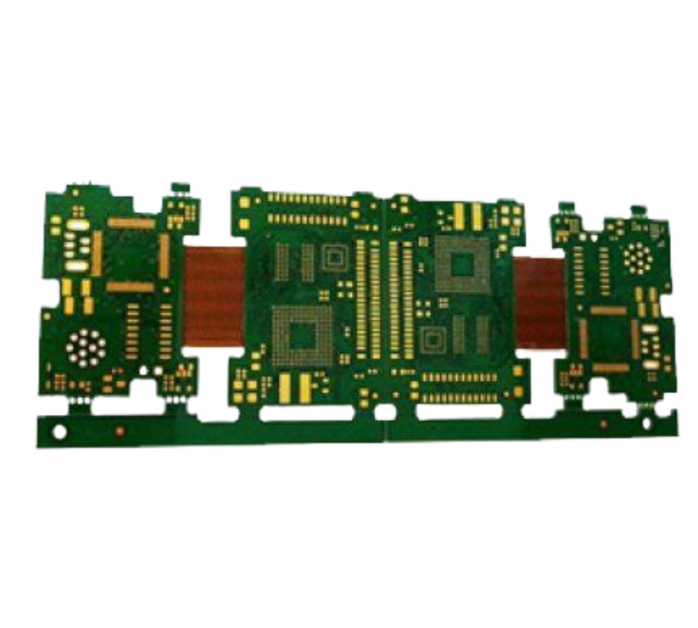
Yes—rigid-flex HDI PCBs integrate rigid and flexible sections, leveraging HDI’s density and flex PCB’s bendability. ShwayPCB manufactures rigid-flex HDI with:
- Rigid sections: FR4 substrate, 4–10 layers, 0.0762mm traces.
- Flexible sections: Polyimide substrate, 2–4 layers, 0.1mm microvias.
This is ideal for devices like smartwatches (rigid main board, flexible strap sensors) or medical endoscopes (rigid control module, flexible probe).
3. What design rules should I follow for HDI PCBs?
To optimize manufacturability and performance:
- Trace Width/Spacing: Minimum 0.0762mm (3mil) for rigid HDI, 0.1mm (4mil) for flexible HDI (per IPC-2226).
- Microvia Placement: Keep microvias ≥0.1mm away from trace edges and ≥0.2mm apart to avoid copper lifting.
- Layer Stackup: Use sequential lamination for multi-layer HDI; avoid crossing microvias between non-adjacent layers.
- DFM Review: Partner with ShwayPCB early—their engineers provide DFM feedback to reduce costs (e.g., optimizing microvia count) and improve yield.
4. How long does HDI PCB Manufacturing take compared to traditional PCBs?
HDI production takes 2–3 days longer than traditional PCBs due to laser drilling and sequential lamination, but lead times remain competitive:
- Prototypes (1–50 units): 5–7 days (HDI) vs. 3–5 days (traditional).
- Low-Volume (100–1k units): 10–14 days (HDI) vs. 7–10 days (traditional).
- High-Volume (10k+ units): 2–3 weeks (HDI) vs. 1–2 weeks (traditional).
ShwayPCB offers expedited HDI prototyping (3–4 days) for time-critical projects (e.g., medical device launches).
5. What quality certifications should I look for in an HDI PCB manufacturer?
Prioritize manufacturers with:
- IPC Certifications: IPC-6012 (performance), IPC-A-600 (acceptability), IPC-2226 (design).
- Industry-Specific Certifications: ISO 13485 (medical), IATF 16949 (automotive), MIL-STD-883H (aerospace).
- ShwayPCB Credentials: All HDI PCBs meet these standards, with full documentation (test reports, CoCs) provided for regulatory audits.
6. Conclusion
HDI PCBs outperform traditional PCBs in miniaturization, density, and performance—making them indispensable for 5G, medical, and automotive innovations. Their unique features (microvias, fine traces) and specialized HDI PCB Manufacturing processes (laser drilling, sequential lamination) address the most demanding design challenges, while their applications span consumer electronics to aerospace.
ShwayPCB’s expertise in PCB manufacturing process and board types includes rigid, flexible, and RF HDI PCBs—with capabilities to produce 0.0762mm traces, 0.1mm microvias, and multi-layer designs up to 12 layers. Whether you need prototypes for a medical wearable or high-volume production for 5G routers, our team provides DFM optimization, rigorous testing, and on-time delivery to meet your goals.
To discuss your HDI PCB design, request a technical consultation, or get a customized quote, contact ShwayPCB at yuan@shwaypcb.com. For detailed specifications on our HDI capabilities—including material options and testing protocols—visit our dedicated PCB manufacturing page.

- Sign Up For Newsletter
-
Join 60.000+ subscribers and get a new discount coupon on every Saturday.
Copyright © 2005-2025 ShwayPCB : PCB Fabrication and Assembly Manufacturer. All Rights Reserved. POWERED BY UEESHOP


- Sign Up For Newsletter
-
Join 60.000+ subscribers and get a new discount coupon on every Saturday.
Copyright © 2005-2025 ShwayPCB : PCB Fabrication and Assembly Manufacturer. All Rights Reserved. POWERED BY UEESHOP