We use cookles to Improve your online experience. By continuing browsing this website, we assume you agree our use of cookies.

HDI PCB vs. Standard PCB Board: Key Technical Differences
September 2nd, 2025
235 views
HDI PCB vs. Standard PCB Board: Key Technical Differences
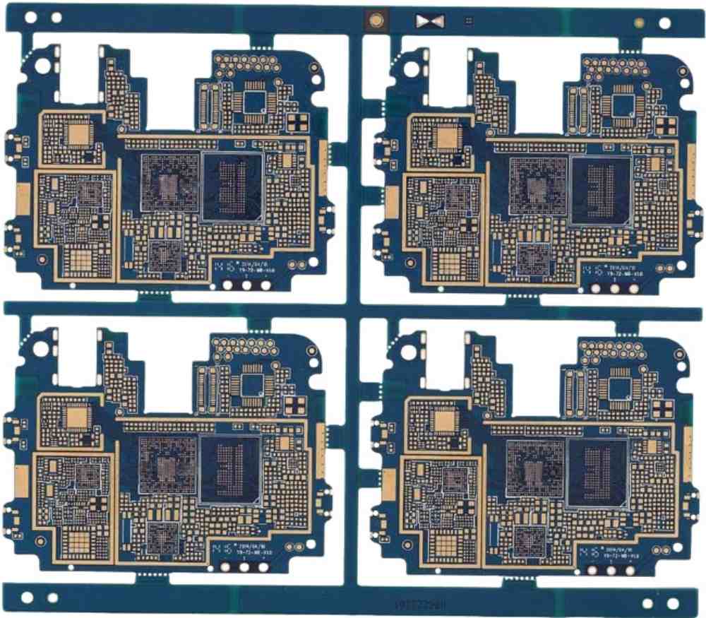
The terms "HDI PCB" and "standard PCB board" are often used interchangeably, but they represent distinct technologies tailored to different design needs. A standard PCB board (also called a "traditional PCB") relies on larger through-holes, wider traces, and simpler layer integration—ideal for low-to-medium complexity devices like power supplies or basic sensors. In contrast, an HDI PCB (High-Density Interconnect PCB) uses microvias, fine-pitch components, and advanced lamination techniques to enable miniaturization, high-frequency performance, and dense component packing—critical for 5G smartphones, medical wearables, and automotive ADAS modules.
To choose the right technology for your project, it’s essential to understand their differences in design, manufacturing, performance, and cost. This guide compares HDI PCBs and standard PCB boards across 8 technical dimensions, with insights from ShwayPCB—a leader in PCB manufacturing process and board types.
1. Design Geometry: Trace Width, Spacing, and Via Size
The most fundamental difference between HDI PCBs and standard PCBs lies in their design geometry—HDI’s finer features enable far higher density.
|
Design Parameter
|
Standard PCB Board
|
HDI PCB
|
|
Trace Width
|
≥0.127mm (5mil); typical 0.152mm (6mil)
|
≤0.1016mm (4mil); down to 0.0762mm (3mil)
|
|
Trace Spacing
|
≥0.127mm (5mil)
|
≤0.1016mm (4mil); down to 0.0762mm (3mil)
|
|
Via Type & Diameter
|
Through-holes (≥0.3mm/12mil)
|
Microvias (≤0.15mm/6mil); blind/buried vias
|
|
Component Pitch Support
|
≥0.5mm; limited to 0402 passives
|
≤0.4mm; supports 01005 passives, 0.3mm-pitch BGAs
|
Technical Rationale
Standard PCBs use larger traces and through-holes because they rely on older, less precise manufacturing equipment (e.g., mechanical drills). HDI PCBs, by contrast, leverage laser drilling and high-precision SMT machines to create microvias and fine traces—freeing up 40–60% of surface area for components. For example:
- A standard PCB board for a basic IoT sensor might use 0.152mm traces and 0.3mm through-holes, requiring a 50mm × 50mm board.
- An HDI PCB for the same sensor could use 0.0762mm traces and 0.1mm microvias, fitting the design into a 25mm × 25mm board—half the size.
ShwayPCB’s HDI PCB Manufacturing capabilities include UV laser drilling for 0.1mm microvias and 5MP AOI systems to ensure trace accuracy—critical for maintaining yield with fine geometries.
2. Manufacturing Processes: From Drilling to Lamination
HDI PCBs require specialized manufacturing processes that standard PCBs do not—these processes enable their fine features but add complexity and cost.
|
Manufacturing Step
|
Standard PCB Board
|
HDI PCB
|
|
Drilling Method
|
Mechanical drills (≥0.3mm diameter)
|
Laser drilling (UV/CO₂) for microvias (≤0.15mm)
|
|
Lamination Technique
|
Mass lamination (all layers at once)
|
Sequential lamination (layer-by-layer)
|
|
Plating Requirements
|
Basic electroless + electrolytic plating (20–25μm)
|
High-precision pulse plating (20–35μm) for microvias
|
|
Inspection Tools
|
2D AOI, basic continuity testing
|
3D AOI, 3D X-ray, TDR impedance testing
|
Technical Rationale
- Drilling: Mechanical drills cannot create holes smaller than 0.3mm, so standard PCBs are limited to through-holes. HDI PCBs use UV lasers to drill microvias, achieving ±0.005mm placement accuracy—essential for aligning vias with fine traces.
- Lamination: Standard PCBs use mass lamination, which is cost-effective but causes alignment errors (±0.05mm) in multi-layer designs. HDI PCBs use sequential lamination, adding layers one at a time with automated optical alignment (AOA)—achieving ±0.01mm alignment for microvias and blind vias.
- Testing: Standard PCBs only require basic inspection to catch surface defects. HDI PCBs need 3D X-ray to verify microvia plating integrity and TDR testing to ensure impedance control—ShwayPCB includes these tests as standard for all HDI orders, achieving 99.5% first-pass yield (FPY) vs. 97% for standard PCBs.
For example, ShwayPCB’s sequential lamination process enables 8-layer flexible HDI PCB designs (used in medical endoscopes) that standard PCB manufacturers cannot produce—flexible standard PCBs are limited to 2 layers and large traces.
3. Performance: Signal Integrity, Thermal Management, and Reliability
HDI PCBs outperform standard PCBs in high-frequency, high-power, and mission-critical applications—their design minimizes signal loss and heat buildup.
|
Performance Metric
|
Standard PCB Board
|
HDI PCB
|
|
High-Frequency Performance
|
Limited to <1GHz (high signal loss)
|
Supports up to 40GHz (low loss: <0.2dB/inch at 28GHz)
|
|
Thermal Conductivity
|
Low (etched traces, few thermal vias)
|
High (solid copper planes, filled thermal vias)
|
|
Reliability (Field Failure Rate)
|
1–2% (consumer electronics)
|
<0.5% (medical/automotive: <0.1%)
|
|
EMI Susceptibility
|
High (poor ground plane integration)
|
Low (dedicated ground planes, microvia ground grids)
|
Technical Rationale
- Signal Integrity: Standard PCBs have long through-hole stubs that cause signal reflections at frequencies >1GHz. HDI PCBs use microvias to eliminate stubs and controlled-impedance traces (±5% tolerance)—critical for RF HDI PCB applications like 5G and radar. ShwayPCB’s RF HDI designs achieve 25% lower signal loss than standard RF PCBs.
- Thermal Management: Standard PCBs use etched traces that dissipate heat poorly, leading to hotspots. HDI PCBs use solid copper planes and filled thermal vias (4+ per 1W component) to transfer heat—reducing component temperatures by 15–20°C. For automotive BMS, this extends battery life by 10% vs. standard PCBs.
- Reliability: Standard PCBs have higher field failure rates due to larger solder joints and less precise manufacturing. HDI PCBs use smaller, more robust microvias and undergo stricter testing—ShwayPCB’s medical HDI PCBs meet ISO 13485 and have a <0.1% failure rate, compared to 1% for standard medical PCBs.
4. Applications: Which Technology Fits Your Device?
HDI PCBs and standard PCBs serve distinct application niches—choosing the right one depends on complexity, size, and performance needs.
|
Application Category
|
Standard PCB Board Use Cases
|
HDI PCB Use Cases
|
|
Consumer Electronics
|
Basic toys, power supplies, remote controls
|
5G smartphones, smartwatches, wireless earbuds
|
|
Medical Devices
|
Simple thermometers, blood pressure monitors
|
Wearable ECGs, endoscopes, implantable sensors
|
|
Automotive
|
Basic lighting controls, radio units
|
ADAS radar, BMS, infotainment systems
|
|
Industrial
|
Simple sensors, relay controls
|
IoT gateways, industrial robots, 5G industrial routers
|
Real-World Examples
- Standard PCB: A basic remote control uses a 2-layer standard PCB with 0.152mm traces and 0.3mm through-holes—cost-effective and sufficient for low-complexity needs.
- HDI PCB: A 5G smartphone’s main board uses an 8-layer HDI PCB with 0.0762mm traces, 0.1mm microvias, and 0.3mm-pitch BGAs—enabling integration of a 5G modem, AI processor, and wireless charging in a slim enclosure. ShwayPCB manufactures these HDI boards at scale (1M+ units/month), meeting the smartphone brand’s strict size and performance requirements.
5. Cost: Upfront vs. Long-Term Value
HDI PCBs have higher upfront costs than standard PCBs, but they deliver long-term savings for complex or high-volume applications.
|
Cost Factor
|
Standard PCB Board
|
HDI PCB
|
|
Prototype Cost (10 units)
|
\(50–\)100
|
\(150–\)300
|
|
High-Volume Cost (100k units)
|
\(0.50–\)2.00/unit
|
\(1.00–\)3.50/unit
|
|
Rework Cost
|
\(500–\)1,000/batch
|
\(1,000–\)2,000/batch (but lower frequency: <1% of batches)
|
|
Total Cost of Ownership (TCO)
|
Higher for complex designs (due to size/materials)
|
Lower for complex designs (smaller size, fewer failures)
|
Cost Rationale
- Upfront Cost: HDI PCBs cost more due to laser drilling, sequential lamination, and advanced testing. For low-complexity designs (e.g., remote controls), standard PCBs are more cost-effective.
- Long-Term Value: For complex designs, HDI’s smaller size reduces enclosure costs (30–50% savings) and lower failure rates cut warranty costs (20–30% savings). For example, an IoT sensor manufacturer switched from standard PCBs to ShwayPCB’s HDI PCBs—upfront cost increased by 20%, but TCO decreased by 25% due to smaller enclosures and fewer field failures.
6. FAQ: HDI PCB vs. Standard PCB Board
1. When should I choose a standard PCB board instead of an HDI PCB?
Choose a standard PCB if:
- Your design has low complexity (fewer than 50 components, no fine-pitch parts).
- You do not need miniaturization (board size >50mm × 50mm is acceptable).
- Your application operates at low frequencies (<1GHz) with no strict signal integrity requirements.
Examples: Basic remote controls, power supplies, simple toys.
2. Can a standard PCB manufacturer produce HDI PCBs?
No—most standard PCB manufacturers lack the specialized equipment (UV lasers, sequential lamination presses, 3D X-ray machines) and expertise to produce HDI PCBs. Attempting to manufacture HDI designs with standard equipment leads to high defect rates (>5%) and failed performance tests. ShwayPCB’s HDI PCB Manufacturing facilities are purpose-built for HDI, with 12 laser drilling machines and 8 sequential lamination presses.
3. Are HDI PCBs compatible with standard SMT assembly lines?
Yes—HDI PCBs use standard SMT components (e.g., BGAs, passives) but require high-precision SMT machines (±0.015mm accuracy) to place fine-pitch parts. ShwayPCB’s SMT lines include Yamaha YSM40R machines, which handle 01005 passives and 0.3mm-pitch BGAs with 99.8% placement accuracy—compatible with HDI’s dense designs.
4. Can HDI PCBs replace all standard PCBs?
No—standard PCBs remain the best choice for low-complexity, cost-sensitive applications. HDI PCBs are only justified if your design requires:
- Miniaturization (board size <50mm × 50mm).
- High-frequency performance (>1GHz).
- Fine-pitch components (≤0.4mm).
- Mission-critical reliability (medical/automotive).
5. How does ShwayPCB help me decide between HDI and standard PCBs?
ShwayPCB offers free DFM (Design for Manufacturability) reviews to evaluate your design:
- For standard PCB candidates: We confirm if your design can be produced cost-effectively with standard processes.
- For HDI candidates: We provide a detailed HDI design roadmap, including trace/via recommendations and cost estimates.
For example, a client’s industrial sensor design was initially specified for HDI, but ShwayPCB’s DFM review showed a 2-layer standard PCB could meet requirements—saving the client 40% on production costs.
7. Conclusion
The choice between HDI PCBs and standard PCB boards depends on your design’s complexity, size, performance, and cost needs. Standard PCBs are cost-effective for low-complexity, low-frequency applications, while HDI PCBs excel in miniaturized, high-performance, or mission-critical devices—leveraging HDI PCB Manufacturing processes like laser drilling and sequential lamination to deliver unmatched density and reliability.
ShwayPCB’s expertise in PCB manufacturing process and board types includes both standard and HDI PCBs—our team helps you select the right technology and optimize your design for cost and performance. Whether you need a standard PCB for a remote control or an 8-layer RF HDI PCB for 5G radar, we deliver consistent quality and on-time delivery.
To discuss your design, request a DFM review, or get a customized quote, contact ShwayPCB at yuan@shwaypcb.com. For more details on our HDI and standard PCB capabilities—including material options and testing protocols—visit our dedicated PCB manufacturing page.

Copyright © 2005-2025 ShwayPCB : PCB Fabrication and Assembly Manufacturer. All Rights Reserved. POWERED BY UEESHOP


Copyright © 2005-2025 ShwayPCB : PCB Fabrication and Assembly Manufacturer. All Rights Reserved. POWERED BY UEESHOP