We use cookles to Improve your online experience. By continuing browsing this website, we assume you agree our use of cookies.
USD
USD

ALL CATEGORIES
- UWB base station ranging system
- Millimeter wave radar module
- Industrial 1000Mbps Switch Module
- Industrial grade 100Mbps module
- Image Transmission Module
- Industrial Motherboard
- Audio amplifier module
- Power module(DC-DC/AC-DC/High Voltage Power Module)
- learning development boards
- Power temperature measurement module
Green PCB Assembly: Sustainable Materials & Eco-Friendly Processes
By ShwayPCB
August 15th, 2025
211 views
Green PCB Assembly: Sustainable Materials & Eco-Friendly Processes
In an era of increasing environmental awareness, the electronics manufacturing industry is under growing pressure to reduce its ecological footprint. For PCB Prototype Assembly, this shift has given rise to “green PCB assembly”—a set of practices focused on sustainable materials, energy-efficient processes, and reduced waste. Unlike traditional methods, which rely on hazardous chemicals, non-recyclable substrates, and energy-intensive production, green assembly prioritizes environmental responsibility without compromising performance or reliability.
This article explores the principles of green PCB assembly, highlighting sustainable materials, eco-friendly processes, and their impact on both the environment and product quality. We’ll also address common questions about green prototyping and explain how ShwayPCB integrates these practices into its services. By the end, you’ll understand why green PCB assembly is not just a trend but a critical step toward a more sustainable electronics industry.
The Environmental Impact of Traditional PCB Assembly
To appreciate the value of green PCB assembly, it’s essential to recognize the environmental challenges posed by traditional PCB Prototype Assembly processes:
1. Hazardous Materials
- Heavy Metals: Traditional PCBs often contain lead (in solder), cadmium (in plating), and mercury (in some components)—all of which are toxic and can leach into soil or waterways if not disposed of properly.
- Volatile Organic Compounds (VOCs): Etching processes use solvents like trichloroethylene and acetone, which release VOCs into the atmosphere, contributing to air pollution and smog.
- Acids and Alkalis: Etching solutions (e.g., ferric chloride, ammonium persulfate) are corrosive and require specialized disposal to prevent environmental contamination.
2. Energy Consumption
Traditional PCB manufacturing is energy-intensive:
- Substrate Production: FR-4, the most common PCB substrate, requires high-temperature processing of fiberglass and epoxy resins, consuming large amounts of fossil fuel-derived energy.
- Etching and Plating: These steps involve pumps, heaters, and ventilation systems that run continuously, increasing carbon emissions.
- Transportation: Sourcing materials from global suppliers (e.g., copper from Chile, fiberglass from China) adds to the carbon footprint via shipping and logistics.
3. Waste Generation
- Material Waste: Subtractive etching processes remove up to 90% of the copper cladding from substrates, resulting in large volumes of copper-rich waste that is often landfilled or incinerated.
- Chemical Waste: Spent etching solutions, cleaning agents, and solder fluxes require costly treatment to meet environmental regulations, with improper disposal leading to soil and water contamination.
- E-Waste: Obsolete PCBs contribute to the growing e-waste crisis—globally, over 50 million metric tons of e-waste are generated annually, with only 17% recycled properly.
These impacts have driven regulatory bodies to impose stricter standards (e.g., RoHS, REACH) and pushed manufacturers to adopt greener alternatives.
Sustainable Materials in Green PCB Assembly
Green PCB Prototype Assembly begins with material selection, prioritizing alternatives that reduce toxicity, improve recyclability, and minimize resource depletion:
1. Eco-Friendly Substrates
- Recycled FR-4: Manufacturers like Isola and Ventec offer FR-4 substrates made from recycled fiberglass and epoxy resins, reducing reliance on virgin materials. These substrates meet the same mechanical and electrical specifications as traditional FR-4 but with a 30–40% lower carbon footprint.
- Biodegradable Substrates: For low-temperature, short-lifespan applications (e.g., disposable sensors), substrates made from plant-based materials (e.g., cellulose, starch-based polymers) are emerging. These decompose naturally in landfills, reducing long-term waste.
- Halogen-Free Laminates: Traditional FR-4 contains brominated flame retardants (halogens), which release toxic dioxins when incinerated. Halogen-free alternatives use phosphorus or nitrogen-based flame retardants, which are less harmful to the environment.
- High-Thermal-Conductivity Substrates: Materials like aluminum nitride (AlN) or silicon carbide (SiC) improve heat dissipation, reducing the need for energy-intensive cooling systems in end products.
2. Sustainable Conductive Materials
- Lead-Free Solder: RoHS-compliant solder alloys (e.g., tin-silver-copper, SnAgCu) replace traditional lead-tin solder, eliminating lead toxicity. While lead-free solder requires higher reflow temperatures (increasing energy use slightly), advances in alloy formulations are reducing this gap.
- Recycled Copper: Copper traces made from recycled content (up to 95% recycled copper) have the same conductivity as virgin copper but reduce mining-related environmental damage. Companies like Aurubis supply recycled copper specifically for PCB applications.
- Silver-Clad Copper: For high-frequency designs, silver-clad copper traces reduce material usage compared to solid silver, lowering costs and environmental impact while maintaining performance.
3. Green Component Packaging
- Lead-Free Components: RoHS-compliant resistors, capacitors, and ICs eliminate lead in terminations and internal structures, aligning with green assembly goals.
- Recyclable Packaging: Components supplied in tape-and-reel formats with recycled plastic carriers or paper-based tapes reduce packaging waste. Some manufacturers also offer bulk packaging to minimize single-use plastics.
- Halogen-Free Component Casings: Plastic component housings made from halogen-free polymers (e.g., LCP, PPS) avoid toxic emissions during incineration.
4. Eco-Friendly Adhesives and Coatings
- Water-Based Fluxes: Traditional fluxes use VOC-rich solvents; water-based alternatives reduce air pollution and simplify waste treatment.
- Conformal Coatings from Renewable Resources: Silicone or acrylic conformal coatings derived from plant-based oils (e.g., soy-based acrylics) provide protection while reducing reliance on petroleum.
- UV-Curable Materials: Adhesives and coatings cured with UV light instead of heat reduce energy consumption during processing.
Eco-Friendly Processes in Green PCB Assembly
Sustainable materials alone are insufficient—green PCB Prototype Assembly requires reengineering processes to minimize energy use, waste, and emissions:
1. Lean Manufacturing and Waste Reduction
- Additive Manufacturing: 3D printing of PCBs (as discussed in previous articles) eliminates the waste associated with subtractive etching, using only the material needed for traces and substrates.
- Just-in-Time (JIT) Production: Producing prototypes in small batches on demand reduces overproduction and inventory waste, a key principle of lean manufacturing.
- Closed-Loop Material Recycling: Capturing and recycling copper waste from etching processes reduces landfill disposal and lowers the need for virgin copper mining. Advanced facilities can recover up to 98% of copper from etching solutions.
- Chemical Recycling: Spent fluxes and cleaning agents are treated to remove contaminants, allowing them to be reused in the production process—reducing both waste and material costs.
2. Energy Efficiency
- Renewable Energy Integration: Facilities powered by solar, wind, or hydroelectric energy reduce reliance on fossil fuels. For example, a PCB assembly plant with on-site solar panels can cut carbon emissions by 50–70%.
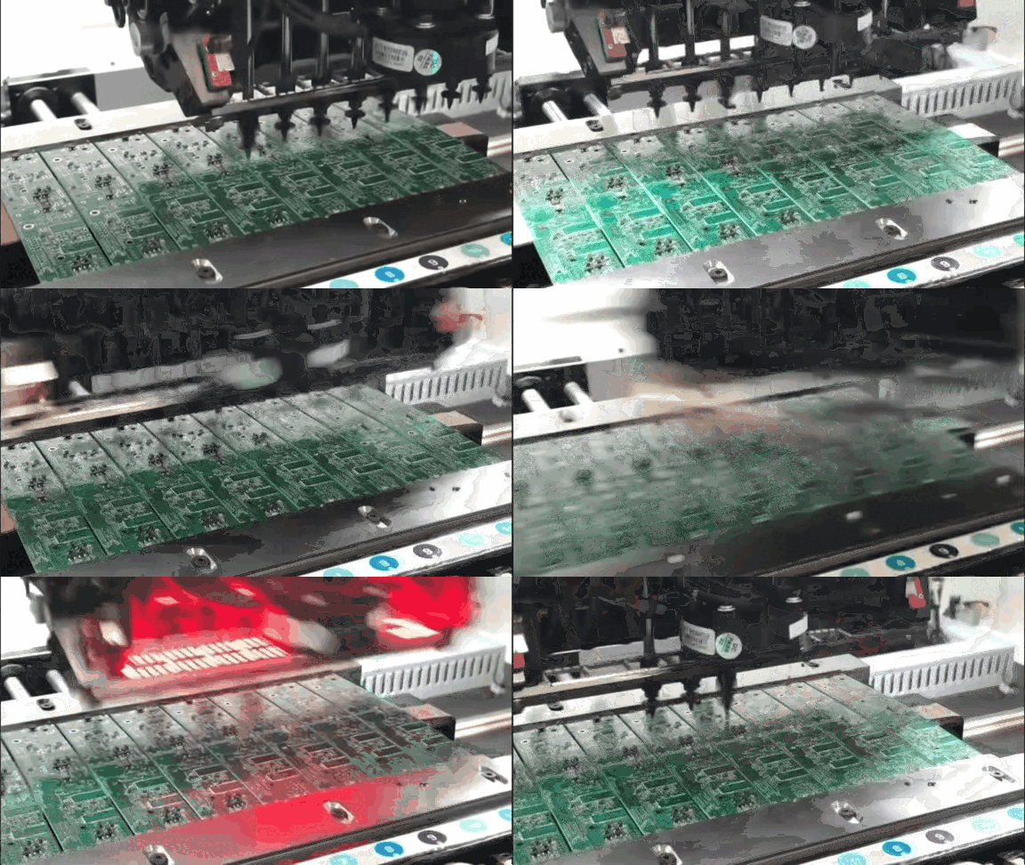
- Energy-Efficient Equipment: Modern pick-and-place machines, reflow ovens, and AOI systems are designed to use 30–40% less energy than older models. Variable-speed drives and heat recovery systems further reduce consumption.
- Process Optimization: Scheduling production to minimize equipment idle time, using high-efficiency lighting, and optimizing heating/cooling systems all contribute to lower energy use.
3. Clean Production Techniques
- Dry Film Etching: This process uses photopolymer films instead of liquid etchants, reducing chemical waste and simplifying handling.
- Plating with Reduced Heavy Metals: Acid copper plating processes are being replaced with more efficient systems that use lower concentrations of heavy metals, reducing both material use and waste.
- Water Conservation: Closed-loop water recycling systems treat and reuse water from cleaning and rinsing steps, reducing freshwater consumption by up to 80% compared to open systems.
4. Green Supply Chain Practices
- Local Sourcing: Using regional suppliers for materials (e.g., copper from North America, substrates from Europe) reduces transportation-related emissions.
- Supplier Audits: Partnering only with suppliers who meet environmental standards (e.g., ISO 14001 certification) ensures sustainability throughout the supply chain.
- Carbon Offsetting: For unavoidable emissions (e.g., long-distance shipping), investing in carbon offset projects (reforestation, renewable energy) helps neutralize the environmental impact.
Benefits of Green PCB Assembly
Adopting green practices in PCB Prototype Assembly delivers multiple benefits, spanning environmental, economic, and reputational gains:
1. Environmental Benefits
- Reduced Toxicity: Eliminating lead, halogens, and VOCs reduces soil, water, and air pollution, protecting ecosystems and human health.
- Lower Carbon Footprint: Energy-efficient processes and renewable energy use reduce greenhouse gas emissions, contributing to global climate goals.
- Conservation of Resources: Recycling materials and reducing waste preserves finite resources (e.g., copper, petroleum) for future generations.
- E-Waste Reduction: Designing PCBs for recyclability (e.g., using easily separable materials) increases the recovery of valuable components at end-of-life.
2. Economic Benefits
- Regulatory Compliance: Meeting standards like RoHS, REACH, and California’s Proposition 65 avoids fines and legal penalties, which can exceed $100,000 for non-compliance.
- Cost Savings: Energy efficiency, waste reduction, and material recycling lower operational costs. For example, water recycling can cut utility bills by 30–50%.
- Market Access: Green PCBs enable access to eco-conscious markets (e.g., European Union, Scandinavian countries) where environmental regulations are strict.
- Brand Reputation: Demonstrating commitment to sustainability enhances brand value, appealing to consumers, investors, and partners who prioritize environmental responsibility.
3. Technical Benefits
- Improved Reliability: Lead-free solder alloys and halogen-free substrates often offer better thermal stability and resistance to corrosion, improving long-term performance.
- Design Flexibility: Sustainable materials like high-thermal-conductivity substrates enable more compact designs by reducing the need for heat sinks.
- Future-Proofing: As environmental regulations tighten, green PCBs are less likely to require redesigns to meet new standards, saving time and resources.
Implementing Green PCB Assembly: Best Practices
For teams looking to adopt green Low-Volume PCB Assembly, follow these guidelines to ensure success:
1. Set Clear Sustainability Goals
- Define Metrics: Establish measurable targets (e.g., “50% recycled copper content,” “20% reduction in energy use”) to track progress.
- Prioritize High-Impact Areas: Focus first on changes with the biggest environmental benefits, such as switching to lead-free solder or implementing recycling programs.
2. Collaborate with Green Suppliers
- Audit Supplier Practices: Verify that material suppliers meet ISO 14001 (environmental management) and have clear sustainability policies.
- Request Environmental Data: Ask for certificates of compliance (e.g., RoHS, halogen-free) and lifecycle assessments (LCAs) of materials to validate their green claims.
3. Optimize Design for Sustainability
- Design for Recyclability: Use standard component sizes and avoid adhesives that make disassembly difficult. Label materials to facilitate recycling at end-of-life.
- Minimize Material Use: Reduce PCB size, use thinner copper traces (where possible), and eliminate unnecessary layers to cut material consumption.
- Select Energy-Efficient Components: Choose low-power ICs and passive components to reduce the energy footprint of the end product.
4. Validate and Certify
- Third-Party Certification: Obtain certifications like ISO 14001 (for environmental management) or EPEAT (for electronic product environmental assessment) to validate green practices.
- Life Cycle Assessment (LCA): Conduct an LCA to quantify the environmental impact of your PCB from raw material extraction to disposal, identifying areas for improvement.
- Continuous Improvement: Regularly review processes and materials, adopting new green technologies as they become available.
FAQ: Green PCB Assembly
Q1: Are green PCBs more expensive than traditional ones?
A1: Initially, yes—sustainable materials and processes can increase costs by 10–20%. However, long-term savings from reduced waste, energy efficiency, and regulatory compliance often offset this premium. As green technologies scale, costs are declining rapidly.
Q2: Do green PCBs compromise performance or reliability?
A2: No. Modern green materials (e.g., lead-free solder, halogen-free substrates) meet or exceed the performance of traditional alternatives. In fact, lead-free solder often has better thermal fatigue resistance, improving reliability in high-temperature applications.
Q3: Can all PCB types be manufactured using green processes?
A3: Most can, including high-frequency, multi-layer, and flexible PCBs. However, some specialized applications (e.g., ultra-high-temperature aerospace PCBs) may still require traditional materials due to limited green alternatives—though this is changing as technology advances.
Q4: How do I verify that a PCB assembly provider is truly “green”?
A4: Look for ISO 14001 certification, which requires a documented environmental management system. Ask for evidence of material sourcing (e.g., recycled content certificates), waste reduction programs, and energy use data. Avoid providers making vague “green” claims without substantiation.
Q5: Are green PCBs recyclable?
A5: Yes, and often more easily than traditional PCBs. Halogen-free substrates and lead-free components simplify recycling, allowing for better recovery of copper, gold, and other valuable materials. Many green assembly providers offer take-back programs for end-of-life PCBs.
Q6: Does green PCB assembly support quick-turn prototypes?
A6: Yes. Most green processes (e.g., lead-free soldering, halogen-free substrates) do not add significant lead time. Reputable providers offer green quick-turn services with delivery times comparable to traditional prototypes.
Q7: What role do regulations play in green PCB assembly?
A7: Regulations like RoHS (restricting hazardous substances) and REACH (controlling chemical use) drive adoption by mandating green practices for products sold in the EU and other regions. Compliance is often a primary motivator for switching to green assembly.
ShwayPCB: Leading the Way in Green PCB Assembly
At ShwayPCB, we are committed to sustainable PCB Prototype Assembly that balances environmental responsibility with performance. Our green practices include:
- Eco-Friendly Materials: Use of recycled copper, halogen-free substrates, and lead-free solder alloys, with full RoHS and REACH compliance.
- Energy-Efficient Facilities: Our production lines are powered by 30% renewable energy, with energy-efficient equipment and heat recovery systems.
- Waste Reduction: Closed-loop recycling of copper and chemicals, with zero hazardous waste sent to landfills.
- Sustainable Supply Chain: Partnerships with ISO 14001-certified suppliers and local sourcing to minimize transportation emissions.
Whether you need a green prototype for a consumer device, medical equipment, or industrial system, we deliver the quality and sustainability you require.
To learn more about our green PCB assembly services or request a quote, contact us at yuan@shwaypcb.com.

- Sign Up For Newsletter
-
Join 60.000+ subscribers and get a new discount coupon on every Saturday.
Copyright © 2005-2025 ShwayPCB : PCB Fabrication and Assembly Manufacturer. All Rights Reserved. POWERED BY UEESHOP


- Sign Up For Newsletter
-
Join 60.000+ subscribers and get a new discount coupon on every Saturday.
Copyright © 2005-2025 ShwayPCB : PCB Fabrication and Assembly Manufacturer. All Rights Reserved. POWERED BY UEESHOP