We use cookles to Improve your online experience. By continuing browsing this website, we assume you agree our use of cookies.

From Concept to Delivery: The Full Process of Turnkey PCB Manufacturing and Assembly
September 3rd, 2025
130 views
From Concept to Delivery: The Full Process of Turnkey PCB Manufacturing and Assembly
Bringing a PCB-based product to life—whether a medical device, industrial controller, or consumer wearable—involves a complex sequence of technical steps. For most teams, coordinating these steps across multiple vendors (design consultants, fabricators, assemblers) leads to miscommunication, delays, and quality gaps. Turnkey PCB Manufacturing and Assembly eliminates these pain points by unifying the entire process under one provider, guiding projects from initial concept to final delivery with consistency, accountability, and efficiency.
This article breaks down the full turnkey process into 7 sequential stages, detailing key activities, technical considerations, and quality checkpoints at each phase. It also highlights how ShwayPCB’s Turnkey PCB Manufacturing and Assembly services streamline workflows for clients across industries, ensuring on-time, compliant, and high-quality outcomes.
1. Stage 1: Concept Validation and Requirements Definition
Before any design work begins, the turnkey provider collaborates with the client to align on project goals and technical constraints—this foundational stage prevents costly rework later.
Key Activities:
- Requirements Gathering:
- Define functional needs (e.g., "The PCB must support Wi-Fi 6 and Zigbee for a smart home hub").
- Specify environmental constraints (e.g., -40°C to +85°C operating temperature for automotive use, IP65 dust/water resistance for industrial sensors).
- Outline regulatory compliance (e.g., ISO 13485 for medical devices, RoHS 3 for consumer electronics).
- Feasibility Analysis:
- Evaluate if the concept is technically achievable (e.g., "Can a 100mm×80mm PCB fit all required components without thermal issues?").
- Assess cost and timeline expectations (e.g., "A 4-layer PCB with SMT BGAs will require 6–8 weeks from design to delivery").
Technical Deliverable:
A Project Requirements Document (PRD) that formalizes functional, environmental, and compliance goals—serving as a roadmap for subsequent stages. For example, ShwayPCB’s team helped a startup refine their wearable PCB concept, adjusting component selection to meet size constraints while maintaining battery life targets.
2. Stage 2: PCB Design and DFM Optimization
Design is critical to manufacturing success—turnkey providers integrate design support and DFM (Design for Manufacturability) reviews to ensure designs are production-ready.
Key Activities:
- Schematic Design:
- Create a circuit schematic (using tools like Altium Designer or KiCad) that maps component connections (e.g., microcontroller to sensors, power management IC to battery).
- Select components based on availability, cost, and compliance (e.g., choosing RoHS-compliant passives, long-lifecycle microchips for industrial projects).
- PCB Layout Design:
- Arrange components to optimize space (e.g., placing high-heat ICs near vents) and signal integrity (e.g., routing high-speed traces away from power lines to reduce crosstalk).
- Define layer stackup (e.g., 4-layer FR-4 with 1oz copper for power/gnd planes) and design rules (trace width 0.12mm, clearance 0.1mm for standard fabrication).
- DFM Review:
- Turnkey providers use automated tools and engineering expertise to flag issues like:
- Unmanufacturable trace widths (e.g., 0.08mm is too narrow for most fabricators).
- Component placement conflicts (e.g., a 0.3mm-pitch BGA with insufficient clearance from a through-hole connector).
- Thermal hotspots (e.g., a 10W microprocessor without a heat sink footprint).
Technical Deliverable:
Finalized Gerber files, BOM (Bill of Materials), and a DFM report with approved design adjustments. ShwayPCB’s High-Reliability PCB Manufacturing and Assembly includes a 24-hour DFM turnaround for urgent projects, ensuring designs move quickly to fabrication.
3. Stage 3: Component Sourcing and Incoming Quality Control (IQC)
Turnkey providers manage component procurement, leveraging global networks to secure high-quality parts at competitive prices—critical for avoiding counterfeits and delays.
Key Activities:
- Supplier Qualification:
- Source components from ISO 9001-certified distributors (e.g., Digi-Key, Mouser) to ensure traceability to original manufacturers (OCMs).
- For hard-to-find parts (e.g., legacy ICs for industrial upgrades), use Legacy PCB Manufacturing and Assembly expertise to identify compatible replacements or secure stock.
- Bulk Sourcing:
- Negotiate volume discounts (10–20% lower than client-direct sourcing) for high-quantity orders (1k+ units).
- Manage inventory to avoid stockouts (e.g., ordering 10% extra passives to account for assembly waste).
- IQC Inspection:
- 100% visual inspection of components to check for physical damage (e.g., bent pins, cracked packages).
- Dimensional testing (e.g., BGA coplanarity <0.05mm) and solderability testing (per IPC-TM-650) to ensure parts will perform in assembly.
Technical Deliverable:
A validated BOM with sourced components, IQC reports, and certificates of conformance (CoCs) for traceability.
4. Stage 4: PCB Fabrication
Fabrication transforms design files into physical bare PCBs—turnkey providers oversee this precision process to ensure structural and electrical integrity.
Key Activities:
- Material Preparation:
- Select substrate material based on requirements (e.g., FR-4 for standard use, Rogers 4350B for high-frequency RF designs).
- Cut substrates to size (e.g., 150mm×200mm for a consumer PCB) and clean them to remove contaminants.
- Core Fabrication Steps:
- Layer Lamination: Bond copper-clad laminates with prepreg (resin-impregnated fiberglass) under heat (180–220°C) and pressure (300–500 psi) to form multi-layer PCBs.
- Drilling: Use laser or mechanical drills to create vias (0.1mm minimum diameter) for interlayer connectivity.
- Plating: Deposit copper into vias (25μm minimum thickness) to ensure electrical continuity.
- Solder Mask and Silkscreen: Apply solder mask (green, red, or custom color) to protect traces; add silkscreen labels (component IDs, logos) for assembly.
- Quality Checks:
- Electrical Testing (E-Test): Use flying-probe testers to verify continuity and insulation resistance (>100MΩ at 500V DC).
- AOI Inspection: Automated optical inspection detects defects like missing vias, short circuits, or solder mask misalignment.
Technical Deliverable:
Bare PCBs with fabrication test reports (E-test results, AOI images). ShwayPCB’s fabrication partners meet IPC-6012 standards, ensuring PCBs meet industry reliability benchmarks.
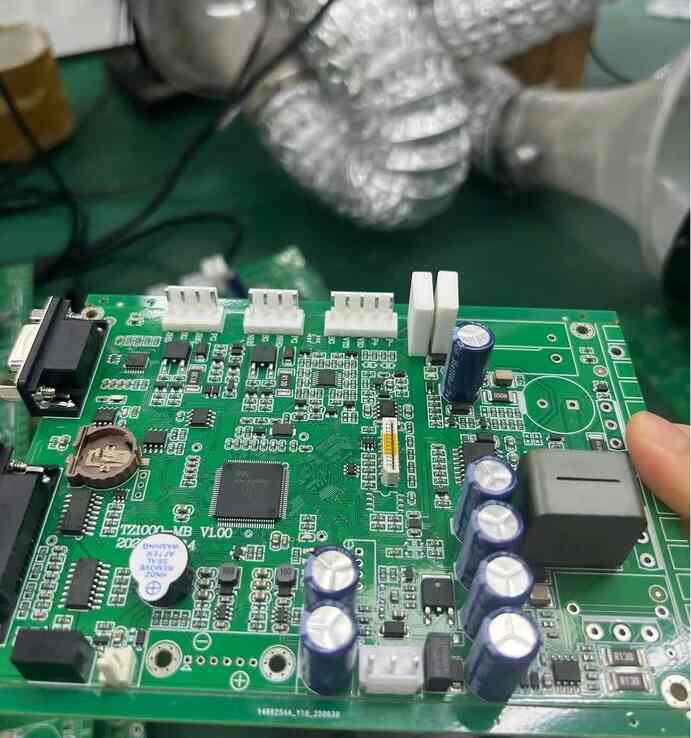
5. Stage 5: PCB Assembly (SMT, Through-Hole, Hybrid)
Assembly populates bare PCBs with components—turnkey providers use automated equipment and skilled technicians to ensure precision and consistency.
Key Activities:
- SMT Assembly (for Miniaturized Components):
- Solder Paste Printing: Use a stencil to deposit solder paste (Type 4/5 for fine-pitch parts) onto PCB pads with ±3% volume accuracy.
- Component Placement: 3D vision-guided machines place SMT components (01005 passives, 0.3mm-pitch BGAs) at speeds up to 100,000 parts per hour.
- Reflow Soldering: Heat PCBs in a nitrogen-enriched oven (O₂ <50ppm) to melt solder paste, forming joints that meet IPC-A-610 standards.
- Through-Hole Assembly (for High-Power Components):
- Insert through-hole components (e.g., transformers, connectors) into PCB holes.
- Post-Assembly Inspection:
- X-Ray Inspection: Check hidden joints (e.g., BGA voids <5% volume) for defects.
- Manual Visual Inspection (MVI): IPC-A-610 certified technicians inspect through-hole solder fillets (75–100% pad coverage) and component alignment.
Technical Deliverable:
Populated PCBs with assembly inspection reports (X-ray images, MVI checklists).
6. Stage 6: Testing, Validation, and Compliance
Turnkey providers conduct comprehensive testing to ensure PCBs meet functional, environmental, and regulatory requirements—critical for avoiding field failures.
Key Activities:
- Electrical Testing:
- ICT (In-Circuit Testing): Verify component values, solder joint integrity, and continuity using a bed-of-nails fixture.
- FCT (Functional Circuit Testing): Simulate real-world operation (e.g., "Test if the IoT sensor transmits data to the cloud," "Verify medical device ECG signal accuracy") using custom test fixtures.
- Environmental Testing:
- Thermal Cycling: -40°C to +85°C for 1,000 cycles (MIL-STD-883H) to test solder joint durability.
- Vibration Testing: 10–20G vibration (ISO 16750-3) for automotive/industrial PCBs.
- Humidity Testing: 85% RH at 85°C for 500 hours (IEC 60068-2-78) for outdoor electronics.
- Regulatory Compliance Testing:
- Medical: IEC 60601-1 electrical safety (leakage current <100μA), ISO 13485 documentation.
- Automotive: AEC-Q100 component qualification, CISPR 25 EMI testing (≤54dBμV/m at 30m).
- Consumer: RoHS 3 compliance, FCC Part 15 EMI testing.
Technical Deliverable:
Test reports (ICT/FCT results, environmental data), compliance certificates, and a final quality summary. ShwayPCB’s Medical PCB Manufacturing and Assembly includes ISO 17025-accredited testing for global regulatory acceptance.
7. Stage 7: Packaging, Logistics, and Post-Delivery Support
The final stage ensures PCBs reach the client in perfect condition, with ongoing support for any post-launch needs.
Key Activities:
- Packaging:
- Use anti-static bags, ESD trays, or custom boxes to protect PCBs from electrostatic discharge (ESD) and physical damage.
- Label packages with part numbers, quantities, and handling instructions (e.g., "Keep Dry," "ESD Sensitive").
- Logistics:
- Coordinate domestic/international shipping (e.g., FedEx, DHL) with tracking and customs documentation (e.g., CE marking for the EU, FDA import permits for medical devices).
- Offer just-in-time (JIT) delivery to reduce client inventory costs.
- Post-Delivery Support:
- Provide rework services for any defective units (e.g., replacing a damaged BGA).
- Assist with design iterations for future production runs (e.g., optimizing component placement for cost savings).
- Maintain traceability records (component lots, test data) for 7+ years for regulatory audits.
Technical Deliverable:
Delivered PCBs, packaging slips, shipping documents, and a post-delivery support contact.
8. FAQ: The Turnkey PCB Manufacturing and Assembly Process
1. How long does the full turnkey process take?
Timelines depend on complexity and volume:
- Prototypes (5–10 units): 5–7 days (design + fabrication + assembly + basic testing).
- Low-Volume Production (100–1k units): 2–3 weeks (includes DFM, sourcing, and compliance testing).
- High-Volume Production (10k+ units): 4–6 weeks (adds process validation and statistical testing).
ShwayPCB’s Turnkey PCB Manufacturing and Assembly offers expedited 2-week service for urgent projects.
2. Can I make design changes mid-process?
Yes—turnkey providers handle changes with minimal disruption:
- Pre-Fabrication: Design tweaks (e.g., adjusting a trace width) add 1–2 days and \(50–\)200.
- Post-Fabrication: Assembly-stage changes (e.g., replacing a resistor value) add 3–5 days and \(100–\)500.
Changes are documented in a formal engineering change order (ECO) for traceability.
3. How do I track my project’s progress?
Turnkey providers offer transparent tracking:
- Dedicated Project Manager: A single point of contact provides weekly updates (or daily for expedited projects).
- Online Portal: Access real-time status (e.g., "Fabrication complete, moving to assembly") and download test reports.
4. What if my PCBs fail after delivery?
Turnkey providers offer warranty and support:
- Warranty: 1–3 years for manufacturing defects (covers solder joints, component failures from assembly).
- Root-Cause Analysis: If failures occur, the provider investigates (e.g., "Field failures due to insufficient solder paste—revised SPI parameters for future runs").
- Rework/Replacement: Defective units are reworked or replaced at no cost during the warranty period.
5. Do turnkey providers handle PCB assembly for mixed SMT/through-hole designs?
Yes—Hybrid PCB Manufacturing and Assembly is a core capability:
- Selective wave soldering targets through-hole pads without damaging SMT components.
- DFM reviews ensure through-hole parts do not block SMT placement paths.
9. Conclusion
The turnkey PCB manufacturing and assembly process—from concept to delivery—unifies design, sourcing, fabrication, assembly, and support into a seamless workflow. By partnering with a turnkey provider, teams eliminate vendor coordination headaches, reduce time-to-market by 30–40%, and ensure consistent quality across every stage. For industries where reliability and compliance are critical—medical, automotive, aerospace—this end-to-end approach is not just efficient, but essential.
ShwayPCB’s Turnkey PCB Manufacturing and Assembly services are engineered to guide projects of all sizes and complexities, with a focus on technical excellence, transparency, and client collaboration. Our team works as an extension of yours, ensuring your PCB-based product meets every requirement—from initial concept to final delivery.
To discuss your project’s turnkey journey, request a free feasibility analysis, or get a customized quote, contact ShwayPCB at yuan@shwaypcb.com. For detailed case studies of projects we’ve guided from concept to delivery, visit our dedicated Turnkey PCB Manufacturing and Assembly page.

Copyright © 2005-2025 ShwayPCB : PCB Fabrication and Assembly Manufacturer. All Rights Reserved. POWERED BY UEESHOP


Copyright © 2005-2025 ShwayPCB : PCB Fabrication and Assembly Manufacturer. All Rights Reserved. POWERED BY UEESHOP