
Comprehensive Analysis of PCB Material Classification and Special Performance PCB Boards: Worry-Free Material Selection
Classification by Substrate Material
Phenolic Paper-Based Laminates (FR-1, FR-2)
Composition and Structure:
Uses phenolic resin as the binder and paper-based fiber cloth as the reinforcing material. Phenolic resin offers good insulation and heat resistance, while the paper-based fiber cloth provides mechanical strength to the board.
Performance Characteristics:
Advantages: Low cost, good machinability, suitable for simple circuit boards with low performance requirements, such as basic control boards in consumer electronics.
Disadvantages: Relatively poor heat resistance, moisture resistance, and electrical performance. Prone to performance degradation or damage in high-temperature or high-humidity environments.
Applications:
Primarily used in cost-sensitive, low-performance electronics, such as radios and calculators.
Epoxy Glass Cloth-Based Laminates (FR-4)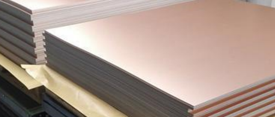
Composition and Structure:
Composed of epoxy resin and glass fiber cloth. Epoxy resin provides excellent adhesion, chemical resistance, and electrical performance, while glass fiber cloth imparts high strength and good dimensional stability.
Performance Characteristics:
Advantages: High mechanical strength, good electrical performance, heat resistance, and moisture resistance. The most widely used PCB substrate material.
Disadvantages: Relatively high cost. In high-frequency applications, dielectric constant and loss may affect signal transmission.
Applications:
Widely used in various electronics, including computers, communication devices, and industrial control equipment.
Polytetrafluoroethylene (PTFE)-Based Laminates
Composition and Structure:
Mainly made of polytetrafluoroethylene (PTFE), often with fillers added to improve machinability and mechanical properties. PTFE's unique molecular structure provides exceptional chemical stability and electrical performance.
Performance Characteristics:
Advantages: Extremely low dielectric constant and loss, significant advantages in high-frequency, high-speed signal transmission. Good chemical corrosion resistance and high-temperature performance.
Disadvantages: High cost, difficult to process, requiring specialized equipment and processes.
Applications:
Mainly used in high-frequency communication equipment, satellite communications, radar, etc.
Ceramic Substrates
Composition and Structure:
Common ceramic substrate materials include aluminum oxide (Al₂O₃) and aluminum nitride (AlN). Ceramic materials exhibit unique crystalline structures, providing excellent physical and chemical properties.
Performance Characteristics:
Advantages: Extremely high thermal conductivity, enabling rapid heat dissipation, suitable for high-power electronic devices. Good insulation performance, mechanical strength, and chemical stability (corrosion-resistant).
Disadvantages: Brittle, difficult to machine, and relatively high cost.
Applications:
Primarily used in high-power LED lighting, power electronics, automotive electronics, etc.
Classification by Flame Retardancy
Flame-Retardant Laminates
Classification Criteria:
According to the UL94 standard, flame-retardant laminates are classified into V-0, V-1, V-2, etc. V-0 rated materials offer the highest flame retardancy, self-extinguishing within 10 seconds after flame removal, with no ignition of cotton by burning drips. V-1 rated materials self-extinguish within 30 seconds, while V-2 rated materials also self-extinguish within 30 seconds but may ignite cotton with burning drips.
Common Types:
Most commonly used PCB substrates, such as FR-4, FR-1, and FR-2, are available in flame-retardant versions.
Applications:
Widely used in various electronics with fire safety requirements, such as computers, communication devices, and household appliances.
Non-Flame-Retardant Laminates
Characteristics:
Non-flame-retardant laminates exhibit rapid flame spread and poor self-extinguishing properties when burned, posing significant safety hazards.
Applications:
Due to low safety performance, non-flame-retardant laminates are increasingly rare in electronics applications. They are mainly used in special occasions or temporary products with low fire safety requirements.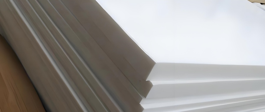
Classification by Special Performance
High-TG Laminates
Definition:
TG (Glass Transition Temperature) refers to the temperature at which a polymer material transitions from a glassy state to a rubbery state. High-TG laminates typically have a TG value above 170°C, compared to the 130–150°C of standard FR-4.
Performance Characteristics:
Higher heat resistance and dimensional stability, less prone to deformation at high temperatures, ensuring electrical and mechanical performance of the circuit board.
Applications:
Primarily used in electronics operating in high-temperature environments, such as automotive electronics, aerospace electronics, and industrial control equipment.
Metal-Based Substrates
Structure:
Typically consist of a metal base layer (e.g., aluminum, copper), an insulating layer, and a circuit layer. The metal base provides excellent heat dissipation, the insulating layer isolates the metal base from the circuit layer, and the circuit layer is used for wiring.
Performance Characteristics:
Excellent heat dissipation, effectively reducing the operating temperature of electronic components and improving product reliability and lifespan. The metal base also provides mechanical strength and shielding properties.
Applications:
Widely used in high-power LED lighting, power modules, automotive electronics, etc.
Classification by Special Performance
High-Frequency Laminates
Principles and Characteristics:
High-frequency laminates are specifically designed for high-frequency signal transmission, with key characteristics including low dielectric constant (Dk) and low dissipation factor (Df). The dielectric constant affects signal propagation speed, while the dissipation factor determines energy loss during signal transmission. Low Dk and Df reduce signal delay, attenuation, and distortion, ensuring the integrity and stability of high-frequency signals.
Common Types:
PTFE-Based High-Frequency Laminates: As previously mentioned, PTFE-based substrates excel in high-frequency applications due to their extremely low dielectric constant and dissipation factor. However, PTFE materials have a relatively high coefficient of thermal expansion (CTE) and weaker adhesion to copper foil, requiring special processing techniques such as plasma treatment to enhance interlayer bonding.
Hydrocarbon-Based High-Frequency Laminates: These laminates use hydrocarbon resins as the matrix, offering good thermal stability, mechanical properties, and dielectric performance. They are more cost-effective than PTFE-based substrates and have better machinability, making them advantageous in high-frequency applications with strict cost and processing requirements.
Ceramic-Filled High-Frequency Laminates: By adding ceramic fillers to matrices like epoxy resin, these laminates effectively reduce dielectric constant and dissipation factor while improving thermal conductivity and dimensional stability. They combine the good machinability of epoxy resin with the high performance of ceramic materials, suitable for applications requiring both thermal management and signal transmission performance.
Applications:
Widely used in 5G communication base stations, satellite communications, radar systems, high-speed digital circuits, etc. For example, in 5G communications, high-frequency laminates are used to fabricate key components such as antennas and RF front-ends to meet the demands of high-speed, high-capacity data transmission.
Flexible Printed Circuits (FPC)
Structure and Materials:
Flexible printed circuits are primarily composed of flexible substrates such as polyimide (PI) or polyester (PET), copper foil, and coverlay. Polyimide, with its excellent high-temperature resistance, chemical corrosion resistance, and mechanical properties, is the most commonly used substrate for FPCs. Polyester is lower in cost but has relatively poor high-temperature resistance. Copper foil is adhered to the substrate via adhesive or directly deposited to form the circuit layer, while the coverlay protects the circuit layer, preventing short circuits and mechanical damage.
Performance Characteristics:
Flexibility: Capable of bending, folding, and twisting to adapt to various complex spatial shapes and installation requirements, providing greater design flexibility for electronic products.
Lightweight and Thin: Light in weight and thin in thickness, facilitating the slim design of electronic products.
Dynamic Reliability: Maintains good electrical and mechanical performance under repeated bending and vibration, suitable for electronic products requiring dynamic movement.
Applications:
Widely used in smartphones, tablets, wearable devices, medical devices, automotive electronics, etc. For example, in smartphones, FPCs are used to connect the display and mainboard, enabling screen folding and bending. In wearable devices, FPCs can conform to body curves, enhancing wearing comfort.
Rigid-Flex PCBs
Structural Characteristics:
Rigid-flex PCBs combine the advantages of rigid and flexible boards, consisting of rigid and flexible regions. The rigid regions use traditional materials like epoxy glass cloth-based laminates to provide mechanical support and stable electrical connections, while the flexible regions employ flexible printed circuits to enable bending and folding. The rigid and flexible regions are connected through special processes to form an integrated whole.
Performance Advantages:
Space Optimization: Maximizes the use of internal space in electronic products, reduces the use of connectors, and lowers product volume and weight.
High Reliability: Minimizes failures caused by loose or poor contact of connectors, improving product reliability and stability.
Design Flexibility: Enables the design of various complex shapes and structures according to actual product requirements, meeting the needs of different application scenarios.
Applications:
Commonly used in aerospace, military electronics, medical devices, high-end consumer electronics, etc. For example, in aerospace, rigid-flex PCBs can be used in the electronic systems of satellites, aircraft, etc., to achieve complex circuit connections and layouts. In medical devices, they can be used in small, high-reliability equipment such as endoscopes and cardiac pacemakers.
Embedded Copper Block PCBs
Structure and Principles:
Embedded copper block PCBs incorporate copper blocks within the PCB structure. The copper blocks are electrically connected to the circuit layers through metalized holes or buried vias. Copper blocks, with their high thermal conductivity, rapidly dissipate heat generated by electronic components, improving heat dissipation efficiency.
Performance Characteristics:
Significantly enhances the heat dissipation capacity of PCBs, effectively reducing the operating temperature of electronic components and extending product lifespan. Additionally, embedded copper blocks increase the mechanical strength of PCBs, improving product reliability.
Applications:
Mainly used in high-power electronic devices such as high-power LED drivers, server power supplies, and power modules in new energy vehicles. In these devices, electronic components generate significant heat, and embedded copper block PCBs meet their heat dissipation requirements.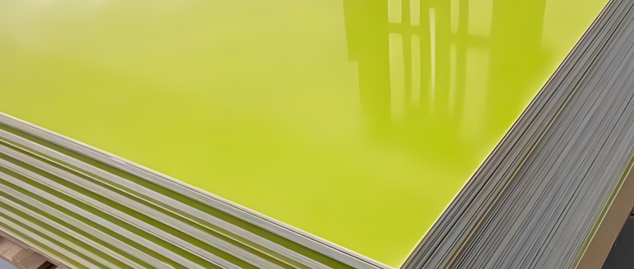
Classification by Special Performance
Electromagnetic Interference (EMI) Shielding Laminates
Principles and Mechanisms:
EMI shielding laminates reduce electromagnetic radiation and enhance shielding against external electromagnetic interference primarily through specialized material formulations and structural designs. On one hand, fillers with electromagnetic shielding capabilities, such as metal powders (silver, copper, etc.) and carbon fibers, may be added to the laminates. These fillers can absorb or reflect electromagnetic waves, thereby reducing the intensity of electromagnetic radiation. On the other hand, the laminate's layered structure and copper foil layout can also contribute to shielding. For example, multi-layer board designs with properly planned ground and power layers can form effective electromagnetic shielding cavities.
Performance Advantages:
Reduced Electromagnetic Radiation: Effectively minimizes electromagnetic radiation generated by electronic products, preventing interference with surrounding electronic devices and meeting Electromagnetic Compatibility (EMC) standards.
Enhanced Interference Resistance: Strengthens the resistance of electronic products to external electromagnetic interference, ensuring stable operation in complex electromagnetic environments and reducing issues such as signal distortion and malfunctions caused by interference.
Applications:
Widely used in fields with high EMC requirements, such as medical devices (e.g., MRI machines, ECG monitors), aerospace electronics, military communication equipment, and industrial automation control systems. In these fields, the normal operation of electronic devices is crucial for personnel safety and system stability, and EMI shielding laminates provide reliable electromagnetic protection.
Low-Loss High-Speed Laminates
Material Characteristics:
Low-loss high-speed laminates employ novel low-loss resin systems and specialized glass fiber cloths. The resin systems feature low dissipation factors and extremely low signal attenuation rates, reducing energy loss during signal transmission. Additionally, optimizing the weaving pattern and structure of the glass fiber cloth minimizes its impact on signal transmission, further improving signal quality.
Performance Characteristics:
Low Signal Loss: Significantly reduces signal attenuation and distortion during high-speed signal transmission, ensuring signal integrity and accuracy.
High-Speed Transmission Capability: Supports higher data transmission rates, meeting the demands of modern electronic products for high-speed data communication, such as 10Gbps, 25Gbps, or even higher rates.
Applications:
Primarily used in high-speed servers, data center switches, high-end routers, high-performance computing equipment, etc. In these devices, large volumes of data need to be transmitted at high speeds within short periods. Low-loss high-speed laminates provide reliable signal transmission guarantees, enhancing the overall performance of the systems.
Chemical-Resistant Laminates
Material Selection and Treatment:
Chemical-resistant laminates typically utilize substrates with excellent chemical resistance and specialized surface treatment processes. For substrates, polymers such as polytetrafluoroethylene (PTFE) and polyetheretherketone (PEEK) may be chosen due to their good tolerance to most chemicals. In terms of surface treatment, special coating technologies may be employed to form a dense protective film on the laminate surface, further enhancing its chemical resistance.
Performance Advantages:
Chemical Erosion Resistance: Capable of operating stably in various chemical environments, including acids, alkalis, and salts, without being corroded or damaged by chemicals, thus preserving the electrical and mechanical properties of the circuit board.
Extended Service Life: Reduces equipment failures and maintenance times caused by chemical corrosion, lowering usage costs and extending the service life of electronic products.
Applications:
Widely used in electronic devices in industries such as chemicals, petroleum, pharmaceuticals, and electroplating. For example, in chemical production processes, electronic devices may come into contact with various corrosive chemicals. Chemical-resistant laminates ensure the normal operation of devices in harsh chemical environments.
High-Thermal-Conductivity Aluminum-Based PCBs
Structure and Thermal Conduction Principle:
High-thermal-conductivity aluminum-based PCBs generally consist of three layers: a circuit layer (copper foil), an insulating layer, and a metal base layer (aluminum plate). The insulating layer employs high-thermal-conductivity insulating materials, such as thermal conductive silicone or thermal conductive epoxy resin, which not only provide electrical insulation but also rapidly conduct heat generated by the circuit layer to the metal base layer. The metal base layer, typically an aluminum plate, possesses good heat dissipation properties, enabling the dissipation of heat into the surrounding environment.
Performance Characteristics:
Efficient Heat Dissipation: Features extremely high thermal conductivity, rapidly conducting heat generated by electronic components away, effectively lowering component operating temperatures, and improving component reliability and lifespan.
High Mechanical Strength: The aluminum plate as the base layer provides good mechanical support, giving the PCB high strength and rigidity to withstand external forces and vibrations.
Applications:
Mainly used in high-power LED lighting, power modules, automotive electronics, etc. In high-power LED lighting, LED chips generate significant heat, and high-thermal-conductivity aluminum-based PCBs can promptly dissipate this heat, ensuring normal LED emission and lifespan. In power modules, they can effectively lower the temperature of power components, improving power efficiency and stability.
Classification by Special Performance (Continued)
Embedded Component Substrates
Structure and Principle:
Embedded component substrates integrate passive components (such as resistors, capacitors, inductors, etc.) directly into or onto the interior of PCB materials, achieving a unified design of components and circuit boards. Through specialized processes, components are fixed at specific positions within the substrate and electrically connected to the circuit layers.
Performance Advantages:
Reduced Size and Weight: Decreases the space occupied by components on the PCB surface, significantly reducing the board's size and weight, and facilitating the miniaturization and lightweight design of electronic products.
Enhanced Integration and Performance: Enables tight integration of components with circuits, shortening signal transmission paths, reducing signal interference and loss, and improving circuit performance and reliability.
Reduced Electromagnetic Interference: By embedding components within the substrate, electromagnetic radiation is effectively minimized, reducing interference with surrounding circuits and other electronic devices.
Applications:
Widely used in high-end electronic products such as smartphones, tablets, high-performance servers, and aerospace electronics. In these products, where stringent requirements are placed on PCB size, weight, and performance, embedded component substrates meet their specific needs.
Electroless Nickel Electroless Palladium Immersion Gold (ENEPIG) Surface Treatment Substrates
Process and Structure:
ENEPIG is a multi-layer surface treatment process that deposits nickel, palladium, and gold layers sequentially onto the surface of PCB copper pads using electroless deposition techniques. The nickel layer, typically 3–6μm thick, acts as a diffusion barrier for copper. The palladium layer, usually 0.05–0.2μm thick, enhances solderability and prevents nickel oxidation. The gold layer, generally 0.02–0.05μm thick, provides excellent oxidation resistance.
Performance Characteristics:
Excellent Solderability and Bondability: Ensures reliable connections between electronic components and PCBs, improving soldering quality and bond strength.
Good Corrosion Resistance: The rational design of each layer and the material properties enable stable performance in harsh environments such as high humidity, high salt spray, or chemical contamination, extending the service life of PCBs.
Suitable for High-Frequency, High-Reliability Applications: In fields like 5G communications, aerospace, and medical electronics, the corrosion resistance and electrical performance of the ENEPIG process meet the high demands placed on PCBs.
Applications:
Primarily used in electronic products requiring high soldering quality, reliability, and corrosion resistance, such as high-end communication equipment, aerospace electronics, and medical electronics.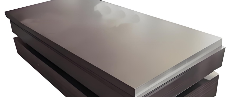
Classification by Special Performance
Carbon Ink Conductive Substrates
Materials and Process:
Carbon ink conductive substrates form conductive pathways on PCB surfaces through methods such as screen printing with carbon ink. The carbon ink primarily consists of carbon powder, resin, and solvents. After high-temperature curing, the carbon particles interconnect to form conductive traces.
Performance Characteristics:
Low Cost: Compared to traditional copper foil traces, carbon ink conductive substrates have relatively lower raw material and processing costs, making them suitable for cost-sensitive mass production.
Good Flexibility: Carbon ink possesses certain flexibility, enabling it to withstand a degree of bending and deformation, suitable for manufacturing flexible or bendable circuit boards.
Resistance Stability: Within a certain temperature and humidity range, the resistance value of carbon ink remains relatively stable. However, it may change under high temperature, high humidity, or after prolonged use.
Applications:
Commonly used in electronic products where conductive performance requirements are not extremely high but cost and flexibility are priorities, such as remote controls, electronic toys, and simple sensors.
Silver Paste Conductive Substrates
Materials and Properties:
Silver paste conductive substrates utilize silver paste as the conductive material. Silver paste is composed of silver microparticles, an organic vehicle, and additives. The silver microparticles exhibit excellent conductivity, while the organic vehicle disperses the silver particles and provides printability. Silver paste conductive traces offer high conductivity and low resistivity, meeting the demands of high-current transmission.
Performance Advantages:
High Conductivity: Silver, being one of the best conductors, enables silver paste conductive substrates to provide superior conductive performance, reducing signal transmission losses and heat generation.
High Printing Precision: Through processes like screen printing, high-precision trace printing can be achieved, suitable for creating minute and complex circuit patterns.
Strong Adhesion: Silver paste exhibits good adhesion to PCB substrates, ensuring the stability and reliability of conductive traces.
Applications:
Widely used in fields such as solar panels, touchscreens, and LED lighting. In solar panels, silver paste conductive traces are used to collect and transmit the current generated by solar cells; in touchscreens, they are used to fabricate sensing electrodes.
Photosensitive Polyimide (PSPI) Substrates
Materials and Principle:
Photosensitive polyimide is a polyimide material with photosensitive properties. During exposure, photosensitive groups undergo chemical reactions, altering the solubility of the material. Through a development process, the unexposed portions are removed, forming the desired circuit pattern. Subsequently, high-temperature curing transforms the polyimide into an insulating layer with excellent mechanical and electrical properties.
Performance Characteristics:
High Resolution: Enables the fabrication of high-precision patterns, suitable for creating fine traces and high-density interconnect PCBs.
Good Insulating Properties: After curing, polyimide exhibits outstanding insulating properties, capable of withstanding high voltages and temperatures.
Chemical Resistance: Possesses good tolerance to most chemicals, enabling stable operation in harsh chemical environments.
Applications:
Primarily used in high-end semiconductor packaging, microelectromechanical systems (MEMS), high-density multilayer PCBs, etc. In semiconductor packaging, PSPI can be used to fabricate redistribution layers (RDLs) and passivation layers, enhancing chip integration and performance.
Liquid Metal-Filled Substrates
Materials and Process:
Liquid metal-filled substrates involve filling microchannels or voids in PCBs with liquid metal (such as gallium-based alloys). Liquid metal possesses good fluidity and conductivity, remaining in a liquid state at room temperature and capable of filling various complex shapes. The filling process typically employs techniques like vacuum infusion or pressure injection to ensure complete filling.
Performance Advantages:
Excellent Heat Dissipation: Liquid metal has extremely high thermal conductivity, rapidly conducting heat away from heat sources and effectively lowering the operating temperature of electronic devices.
Good Conductivity: As a conductive material, liquid metal provides low-resistance electrical connections, reducing signal transmission losses.
Deformability: Under certain conditions, liquid metal can flow and deform, adapting to special application scenarios, such as deformable electronic devices.
Applications:
Suitable for high-power electronic devices, three-dimensional integrated circuits, wearable electronic devices, etc. In high-power LED lighting, liquid metal-filled substrates can be used to fabricate heat dissipation structures, improving LED heat dissipation efficiency; in wearable electronic devices, they can be used to achieve flexible and stretchable electrical connections.
Biocompatible PCB Substrates
Materials and Properties:
Biocompatible PCB substrates are made from materials that are non-toxic, non-irritating, and non-immunogenic to the human body. Common substrates include biodegradable polymers (such as polylactic acid (PLA), polycaprolactone (PCL), etc.) or polymeric materials with good biocompatibility (such as polyurethane). These materials remain stable in the human body environment without releasing harmful substances.
Performance Characteristics:
Biological Safety: No adverse reactions occur when in contact with human tissues and body fluids, suitable for implantable medical electronic devices.
Processability: Can be fabricated using traditional PCB processing techniques, enabling complex circuit designs.
Mechanical Properties: Capable of meeting the mechanical requirements of implantable devices within the human body, such as withstanding certain pressures and frictions.
Applications:
Primarily used in implantable medical electronic devices, such as cardiac pacemakers, neural stimulators, and cochlear implants. These devices require long-term implantation in the human body, and biocompatible PCB substrates ensure the safety and reliability of the devices.
Classification by Special Performance
Ultra-Thin PCB Substrates
Materials and Process:
Ultra-thin PCB substrates typically employ ultra-thin base materials, such as ultra-thin epoxy glass cloth substrates or polyimide films. During fabrication, precise control over processes like lamination and etching ensures that the substrates achieve ultra-thin thicknesses while maintaining excellent performance. For example, during lamination, high-pressure and low-temperature parameters are used to prevent substrate deformation. During etching, the concentration of the etching solution and etching time are optimized to ensure the precision and quality of the traces.
Performance Characteristics:
Extremely Thin and Lightweight: Thicknesses can reach extremely low levels, such as 0.05mm or even thinner, significantly reducing the weight and volume of electronic products and enabling miniaturized and portable designs.
Good Flexibility: Some ultra-thin substrates possess certain flexibility, allowing them to adapt to bending, folding, and other deformation requirements, making them suitable for flexible electronic devices.
Stable Electrical Performance: Despite their thinness, through reasonable material selection and process control, they still maintain good insulation, conductivity, and signal transmission performance.
Applications:
Widely used in electronic products with extremely high requirements for thinness and lightweight design, such as smartwatches, fitness bands, microsensors, and foldable phones. In foldable phones, ultra-thin PCB substrates can be used to fabricate the drive circuits for flexible displays, enabling screen folding functionality.
Flame-Retardant PCB Substrates (Above UL94 V-0 Rating)
Materials and Formulations:
These substrates incorporate special flame retardants into the base materials, such as brominated, phosphorus-based, or nitrogen-based flame retardants. Different flame retardants have distinct mechanisms. Brominated flame retardants decompose at high temperatures to produce hydrogen bromide gas, diluting the concentration of combustible gases and inhibiting the combustion chain reaction. Phosphorus-based flame retardants form phosphoric or polyphosphoric acids during combustion, promoting charring of the substrate surface and creating a heat- and oxygen-insulating char layer. Nitrogen-based flame retardants release non-combustible gases like nitrogen upon decomposition, diluting oxygen concentration.
Performance Advantages:
High Flame Retardancy: Achieving UL94 V-0 or higher flame-retardant standards, they can self-extinguish rapidly when exposed to open flames, effectively preventing the spread of fire and enhancing the safety of electronic products.
Good Thermal Stability: They maintain good physical and chemical properties at high temperatures, are less prone to decomposition and deformation, and ensure the normal operation of circuits.
Environmental Friendliness: With increasing environmental requirements, novel halogen-free flame-retardant substrates are gradually being applied. These substrates meet flame-retardant performance requirements while reducing environmental and human health hazards.
Applications:
Primarily used in electronic products with high safety requirements, such as household appliances (televisions, refrigerators, air conditioners, etc.), industrial control equipment, and automotive electronics. In automotive electronics, PCB substrates with high flame-retardant ratings can reduce the risk of fire in vehicles, ensuring passenger safety.
Radiation-Resistant PCB Substrates
Materials and Protection Mechanisms:
Radiation-resistant PCB substrates utilize materials with radiation-resistant properties, such as special glass fiber cloths and boron-containing polymers. Special glass fiber cloths can reduce radiation-induced damage to the internal structure of the substrates. Boron in boron-containing polymers has good absorption properties for neutron radiation, reducing the impact of radiation on circuit performance. Additionally, the lamination structure and surface treatment processes of the substrates are optimized to enhance their radiation resistance.
Performance Characteristics:
Strong Radiation Resistance: They can operate stably for extended periods in high-radiation environments without being affected by radiation-induced material degradation or circuit failures.
Stable Electrical Performance: In radiation environments, they still maintain good insulation, conductivity, and signal transmission performance, ensuring the normal operation of electronic devices.
Reliable Mechanical Properties: After radiation exposure, the mechanical strength and dimensional stability of the substrates still meet usage requirements, without cracking or deformation.
Applications:
Mainly applied in fields such as aerospace, nuclear energy, and medical radiation. In aerospace, satellites, spacecraft, and other equipment are exposed to cosmic radiation in space, and radiation-resistant PCB substrates can ensure the reliability of their electronic systems. In nuclear energy, control equipment and monitoring instruments in nuclear power plants require radiation-resistant PCB substrates to ensure safe operation in nuclear radiation environments.
Self-Healing PCB Substrates
Healing Mechanisms and Materials:
Self-healing PCB substrates are fabricated using materials with self-healing capabilities. Common self-healing materials include microcapsule-based and intrinsic self-healing materials. In microcapsule-based self-healing materials, microcapsules encapsulate healing agents. When cracks or damage occur in the substrate, the microcapsules rupture, releasing the healing agents to fill the damaged areas and achieve repair through chemical reactions. Intrinsic self-healing materials rely on molecular chain motion and reversible chemical bonds within the material to automatically restore their structure and properties after damage.
Performance Advantages:
Automatic Healing Ability: They can automatically repair minor cracks or damage, extending the service life of PCBs and reducing maintenance costs and downtime.
Improved Reliability: They lower the risk of device damage due to circuit failures, enhancing the reliability and stability of electronic products.
Adaptability to Complex Environments: In harsh working environments, such as high temperatures, high humidity, and strong vibrations, self-healing PCB substrates can better cope with damage and maintain normal operation.
Applications:
Suitable for electronic products with extremely high reliability requirements, such as aerospace electronics, military equipment, and industrial automation control systems. In industrial automation control systems, self-healing PCB substrates can reduce production interruptions caused by circuit failures and improve production efficiency.
Transparent PCB Substrates
Materials and Properties:
Transparent PCB substrates typically use transparent polymeric materials as base materials, such as polymethyl methacrylate (PMMA) and polycarbonate (PC). These materials possess good transparency and optical properties. Through special process treatments, conductive traces are formed on their surfaces. Transparent conductive materials, such as indium tin oxide (ITO) and silver nanowires, can be used for the conductive traces.
Performance Characteristics:
High Transparency: They can maintain high transparency without affecting light transmission, making them suitable for electronic devices requiring light transmission.
Good Conductivity: Transparent conductive materials provide stable conductivity, meeting the basic requirements of circuits.
Strong Processability: They can be fabricated using traditional PCB processing techniques, enabling complex circuit designs and patterning.
Applications:
Mainly used in electronic products requiring a combination of optical and electronic functions, such as transparent displays, smart windows, and touch-sensitive lighting devices. In transparent displays, transparent PCB substrates can be used to connect display units, enabling image display and interactive functionality.
Classification by Special Performance
Antistatic PCB Substrates
Materials and Antistatic Mechanisms:
Antistatic PCB substrates achieve antistatic functionality primarily by incorporating antistatic agents or conductive fillers into the base materials. Antistatic agents can be classified into surfactant-based and polymer-based types. These agents form a conductive layer on the substrate surface, reducing surface resistance and enabling rapid dissipation of static charges. Conductive fillers, such as carbon fibers and metal powders, are uniformly dispersed within the base material to form a conductive network, accelerating the dissipation of static electricity.
Performance Advantages:
Effective Prevention of Static Buildup: They can control the surface resistance of the substrate within a reasonable range (typically 10⁶ - 10⁹Ω), preventing static charges from accumulating to dangerous levels and reducing the risk of electrostatic discharge (ESD) damage to electronic components.
Stable Electrical Performance: While providing antistatic functionality, they do not significantly affect the basic electrical properties of the PCB, such as insulation and conductivity, ensuring normal circuit operation.
Strong Environmental Adaptability: They maintain stable antistatic performance under varying temperature and humidity conditions, making them suitable for diverse and complex working environments.
Applications:
Widely used in the manufacturing of electrostatic-sensitive electronic products, such as semiconductor chip fabrication, electronic component packaging, and precision instrumentation. In semiconductor chip fabrication facilities, antistatic PCB substrates can be used to fabricate circuit boards within equipment, preventing static damage to chips and improving product yield.
High-Frequency, High-Speed, Low-Loss PCB Substrates
Materials and Low-Loss Principles:
These substrates employ materials with low dielectric constants (Dk) and low dissipation factors (Df), such as polytetrafluoroethylene (PTFE), hydrocarbon resins, and liquid crystal polymers (LCP). A low dielectric constant reduces signal delay during transmission, while a low dissipation factor minimizes signal energy loss. Additionally, factors such as the lamination structure of the substrate and the roughness of the copper foil affect signal transmission performance. Optimizing these factors further enhances the high-frequency and high-speed performance of the substrate.
Performance Characteristics:
Excellent High-Frequency, High-Speed Performance: They can maintain signal integrity and stability in high-frequency (typically GHz and above) and high-speed signal transmission environments, reducing signal distortion and crosstalk.
Low Loss: Signal energy loss during transmission is extremely low, improving signal transmission efficiency and reducing system power consumption.
Good Dimensional Stability: They exhibit minimal dimensional changes under temperature variations, ensuring circuit accuracy and reliability.
Applications:
Primarily used in fields with extremely high requirements for signal transmission speed and quality, such as 5G communication equipment, high-speed servers, radar systems, and satellite communications. In 5G base stations, high-frequency, high-speed, low-loss PCB substrates can be used to fabricate key components like RF front-end modules and antennas, meeting the high-speed and large-capacity demands of 5G communications.
High-Temperature, High-Humidity-Resistant PCB Substrates
Materials and Protective Design:
High-temperature, high-humidity-resistant PCB substrates utilize base materials with high temperature and humidity resistance, such as modified epoxy resins and phenolic resins. Special surface treatment processes, such as immersion gold and immersion silver, are employed to enhance oxidation and corrosion resistance. In terms of substrate structure design, waterproof and moisture-proof sealing measures, such as sealing the edges with sealant, are implemented to prevent moisture infiltration.
Performance Advantages:
Outstanding High-Temperature, High-Humidity Resistance: They can operate stably for extended periods in high-temperature (typically tolerating temperatures above 150°C) and high-humidity (relative humidity up to 90% and above) environments without experiencing material softening, deformation, or delamination.
Stable Electrical Performance: Under high-temperature and high-humidity conditions, they maintain low insulation resistance and stable dielectric properties, ensuring normal circuit operation.
Strong Corrosion Resistance: They exhibit good resistance to corrosive substances in the air, such as moisture and salt spray, extending the service life of the PCB.
Applications:
Suitable for electronic products operating in harsh environments, such as outdoor electronic equipment, industrial control equipment, and automotive electronics. In outdoor advertising displays, high-temperature, high-humidity-resistant PCB substrates can withstand direct sunlight, rain immersion, and other harsh conditions, ensuring normal display operation.
Recyclable and Environmentally Friendly PCB Substrates
Materials and Recycling Processes:
Recyclable and environmentally friendly PCB substrates are fabricated using recyclable materials, such as bio-based materials and degradable polymers. During the recycling process, metals (such as copper, gold, silver) and non-metals (such as base materials and resins) in the substrate are separated through physical or chemical methods. Physical methods include crushing, screening, and magnetic separation, while chemical methods utilize solvent dissolution and chemical reactions to achieve material separation and purification.
Performance Characteristics:
Excellent Environmental Performance: They reduce the use of hazardous substances (such as lead, mercury, and cadmium) found in traditional PCB substrates, lowering environmental pollution. Their recyclable nature aligns with sustainable development requirements.
Performance Meets Requirements: While ensuring environmental friendliness, they still meet the basic performance requirements of electronic products for PCBs, such as electrical and mechanical properties, through reasonable material formulations and process designs.
Reduced Resource Consumption: Their recyclable nature enables the reuse of metal and non-metal materials in the substrate, reducing the exploitation and consumption of natural resources.
Applications:
Widely used in electronic product fields with high environmental requirements, such as consumer electronics and office equipment. In laptop manufacturing, the adoption of recyclable and environmentally friendly PCB substrates can reduce the product's environmental impact and enhance the company's environmental image.
Smart Sensing PCB Substrates
Sensing Principles and Integration:
Smart sensing PCB substrates integrate various sensors, such as temperature, humidity, pressure, and acceleration sensors. These sensors can be integrated onto the PCB through printing or surface mounting and electrically connected to the circuit. The sensors can sense real-time changes in physical quantities in the surrounding environment and convert the signals into electrical signals for transmission to subsequent processing circuits.
Performance Advantages:
Multifunctional Sensing: They can simultaneously sense multiple environmental parameters, providing comprehensive environmental information for electronic devices to enable intelligent control and decision-making.
High Integration: Integrating sensors onto the PCB reduces the device's volume and weight, improving system integration and reliability.
Real-Time Response: They can quickly sense environmental changes and respond promptly, meeting the real-time requirements of application scenarios.
Applications:
Primarily used in fields such as smart homes, smart wearables, and industrial IoT. In smart home systems, smart sensing PCB substrates can be used to fabricate control boards for smart appliances, sensing indoor temperature, humidity, and other environmental parameters in real-time to automatically adjust the operating status of appliances and enhance living comfort and convenience.
Classification by Special Performance
Flexible, Transparent, and Conductive PCB Substrates
Materials and Fabrication Processes:
These substrates typically use flexible, transparent polymers as base materials, such as polyethylene terephthalate (PET) or polyethylene naphthalate (PEN). For the conductive layer, in addition to the commonly used indium tin oxide (ITO), novel transparent conductive materials like graphene and metal nanowires (e.g., silver nanowires, copper nanowires) are increasingly being adopted. In terms of fabrication, for graphene, methods such as chemical vapor deposition (CVD) can be used to grow it on the substrate surface, or graphene solutions can be applied to the substrate through coating or printing. For metal nanowires, solution coating methods are generally employed to uniformly apply a solution containing metal nanowires onto the flexible substrate surface, forming a conductive network.
Performance Highlights:
Combination of Flexibility and Transparency: They possess excellent flexibility, allowing for bending, folding, and even twisting operations, while also maintaining good transparency, not affecting light transmission, and meeting special optical and mechanical performance requirements.
Adjustable Conductivity: The conductivity of the substrate can be adjusted within a certain range by varying the type and content of conductive materials, as well as the fabrication process, to suit different application scenarios.
Lightweight and Portable: The overall substrate is very lightweight, facilitating portability and integration into various small, lightweight electronic devices.
Application Areas:
Widely used in fields such as foldable displays, flexible solar cells, and smart wearables (e.g., flexible smartwatches, wearable health monitoring devices). In foldable displays, flexible, transparent, and conductive PCB substrates can serve as the electrode layer for touchscreens, enabling touch functionality without compromising the screen's foldability.
Chemical-Resistant and Highly Insulating PCB Substrates
Materials and Protective Mechanisms:
The base materials selected for these substrates are polymers with excellent chemical resistance, such as polytetrafluoroethylene (PTFE) and polyvinylidene fluoride (PVDF). These materials inherently possess stable chemical structures, offering good resistance to most acids, bases, organic solvents, and other chemicals. To enhance insulation performance, special surface treatments are applied, such as coating with a highly insulating layer or using plasma treatment technologies to improve surface insulation characteristics.
Performance Advantages:
Superior Chemical Resistance: They can operate stably for extended periods in harsh chemical environments containing strong acids, bases, and organic solvents without experiencing material dissolution or corrosion, ensuring circuit reliability.
High Insulation Performance: They exhibit extremely high insulation resistance and dielectric strength, effectively preventing leakage and breakdown phenomena, ensuring the safe operation of electronic devices.
Good Mechanical Properties: While maintaining chemical resistance and high insulation performance, they also possess certain mechanical strength and toughness, capable of withstanding external forces.
Application Scenarios:
Primarily used in electronic devices in industries such as chemicals, petroleum, and pharmaceuticals, such as control instruments in chemical production processes, monitoring equipment on oil drilling platforms, and automation control systems in pharmaceutical workshops. In these environments, electronic devices face erosion from various chemicals, and chemical-resistant and highly insulating PCB substrates provide reliable protection.
Integrated Electromagnetic Shielding and Wave-Absorbing PCB Substrates
Materials and Structural Design:
These substrates employ composite materials with both electromagnetic shielding and wave-absorbing functions. For example, magnetic metal powders (such as ferrite powders, carbonyl iron powders) and conductive fibers (such as carbon fibers, metal fibers) are added to the base material. Magnetic metal powders can absorb electromagnetic waves and convert them into heat for dissipation, while conductive fibers form a conductive network to provide electromagnetic shielding. Meanwhile, through reasonable structural designs, such as multi-layer composite structures or periodic structures, the electromagnetic shielding and wave-absorbing performances are optimized.
Performance Characteristics:
Dual-Function Integration: They possess both electromagnetic shielding functionality, effectively blocking external electromagnetic interference from entering the device, and wave-absorbing functionality, absorbing electromagnetic radiation generated within the device to reduce electromagnetic pollution.
Broadband Characteristics: They can achieve good electromagnetic shielding and wave-absorbing effects over a wide frequency range, adapting to electromagnetic environments of different frequencies.
Lightweight Design: By optimizing materials and structures, the substrates achieve lightweight design while ensuring performance, facilitating integration into various electronic devices.
Application Scenarios:
Suitable for electronic products with extremely high electromagnetic compatibility requirements, such as military communication equipment, aerospace electronic systems, and high-end medical devices. In military communication equipment, integrated electromagnetic shielding and wave-absorbing PCB substrates can ensure normal device operation in complex electromagnetic environments while reducing the device's own electromagnetic radiation to avoid detection by the enemy.
Low-Temperature-Curing, High-Reliability PCB Substrates
Materials and Curing Mechanisms:
These substrates utilize special resin systems, such as epoxy-phenolic resins and cyanate ester resins, which can undergo curing reactions at relatively low temperatures (typically below 150°C). During the curing process, catalysts and accelerators are added to speed up the curing reaction, while curing conditions, such as curing time and heating rate, are controlled to ensure the curing quality and performance of the substrates.
Performance Advantages:
Low-Temperature-Curing Characteristic: They can complete curing at low temperatures, reducing damage to heat-sensitive components and being suitable for the manufacturing processes of some temperature-sensitive electronic products.
High Reliability: The cured substrates possess good mechanical, electrical, and thermal properties, enabling long-term stable operation in various harsh environments and improving the reliability of electronic products.
Energy-Saving and Environmentally Friendly: The low-temperature curing process consumes less energy, reducing production costs and environmental impact.
Application Scenarios:
Primarily used in fields such as LED lighting, automotive electronics, and consumer electronics. In LED lighting, low-temperature-curing, high-reliability PCB substrates can be used to fabricate packaging substrates for LED chips, avoiding high-temperature damage to the chips and improving the lifespan and performance of LED lamps.
Shape-Memory PCB Substrates
Materials and Memory Principles:
Shape-memory PCB substrates use polymer or alloy materials with shape-memory effects as base materials. Shape-memory polymers typically consist of cross-linked polymers that can "remember" their original shape under specific temperature, stress, or other conditions. When deformed by external forces, they can return to their original shape under certain stimuli (such as heating or light exposure). Shape-memory alloys achieve shape-memory functions through phase transitions of the alloy.
Performance Highlights:
Unique Shape-Memory Function: They can change shape according to needs and return to their original shape under specific conditions, providing more possibilities for the design and manufacture of electronic devices.
Stable Electrical Performance: During shape changes, they can still maintain stable electrical performance, ensuring normal circuit operation.
Reusability: The shape-memory function allows the substrates to be deformed and restored multiple times, possessing certain reusability and reducing costs.
Application Areas:
Can be used in electronic devices requiring adaptive deformation or reconfigurability, such as deformable antennas and electronic control systems at the joints of intelligent robots. In deformable antennas, shape-memory PCB substrates can change the antenna's shape according to different communication needs to optimize antenna performance.



