We use cookles to Improve your online experience. By continuing browsing this website, we assume you agree our use of cookies.

Comparing Through-Hole and SMT PCB Assembly: When to Choose Each Method
September 3rd, 2025
213 views
Comparing Through-Hole and SMT PCB Assembly: When to Choose Each Method
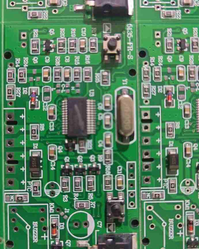
PCB assembly relies on two dominant technologies—through-hole and Surface Mount Technology (SMT)—each with unique strengths that make them suited to specific applications. Through-hole, the traditional method, excels at mechanical robustness and high-power handling, making it indispensable for industrial controls and aerospace systems. SMT, the modern alternative, enables miniaturization and high-density assembly, driving innovation in IoT wearables, smartphones, and consumer electronics.
Choosing the wrong method can lead to costly consequences: using SMT for a high-vibration industrial motor controller may result in 50% higher failure rates, while through-hole for a wearable sensor would make the device too bulky to market. This article compares through-hole and SMT across 6 critical dimensions—mechanical strength, component density, power handling, cost, lead time, and environmental resilience—and provides clear guidance on when to select each. It also highlights how ShwayPCB’s PCB Assembly Services offer both methods, tailoring solutions to client needs from industrial power systems to consumer IoT devices.
1. Mechanical Strength: Through-Hole’s Dominance in High-Stress Environments
Mechanical resilience is critical for applications exposed to vibration, shock, or physical stress—areas where through-hole outperforms SMT.
Through-Hole: Anchored for Durability
- Design Advantage: Component leads pass through drilled PCB holes, creating a "mechanical anchor" that distributes stress across the PCB thickness (0.8–3.2mm). Solder fillets (covering 75–100% of pad area) form a concave bond that resists fatigue cracking.
- Performance Metrics:
- Vibration Resistance: Withstands 10–20G vibration (per IEC 60068-2-6) for 1M cycles—10x more than SMT (100k cycles).
- Shock Tolerance: Survives 50G impact (MIL-STD-883H) without component detachment, compared to SMT’s 20G limit.
- Ideal Applications: Industrial motor controllers, aerospace avionics, heavy machinery sensors—where loose connections cost $10k+/hour in downtime. ShwayPCB’s Industrial PCB Assembly leverages through-hole’s strength for these high-stress use cases.
SMT: Surface-Bonded for Flexibility
- Design Limitation: Components adhere to the PCB surface via solder paste, with no lead penetration. This makes them vulnerable to peeling under vibration or shock.
- Performance Tradeoff:
- Vibration Susceptibility: SMT components (e.g., 0402 resistors) may lift or shift after 50k–100k vibration cycles.
- Mechanical Constraints: Heavy components (>10g, e.g., connectors) require additional adhesives to prevent detachment—adding cost and complexity.
- Mitigation Strategies: Use underfill for critical SMT components (e.g., BGAs in automotive ADAS) to improve mechanical strength, though this increases assembly time by 20%.
2. Component Density and Miniaturization: SMT’s Edge in Compact Designs
Miniaturization and high component density are defining features of modern electronics—areas where SMT is unmatched.
SMT: Dense and Compact
- Design Capabilities:
- Component Size: Supports ultra-small parts (01005 passives: 0.4mm×0.2mm, 0.2mm-pitch BGAs) that through-hole cannot accommodate.
- Double-Sided Assembly: Places components on both PCB sides, doubling density without increasing board size.
- Efficiency Metrics:
- PCB Size Reduction: SMT reduces PCB area by 50–70% vs. through-hole. For example, a wearable fitness tracker uses a 30mm×40mm SMT PCB vs. a 60mm×80mm through-hole equivalent.
- Placement Speed: High-speed SMT machines (e.g., Fuji NXT V) place 60k+ components per hour—10x faster than automated through-hole insertion.
- Ideal Applications: IoT wearables, smartphones, medical implants (e.g., glucose monitors)—where size and weight are critical. ShwayPCB’s High-Density PCB Assembly specializes in SMT for these compact designs.
Through-Hole: Bulky but Reliable
- Design Limitations:
- Component Size: Limited to larger parts (0402+ passives, axial resistors) with leads ≥0.5mm diameter.
- Space Requirements: Leads require drilled holes and pad clearance, increasing PCB size and reducing density.
- Practical Constraints: A through-hole IoT sensor would need a PCB 2–3x larger than an SMT version, making it unfit for wearable or portable devices.
3. Power Handling: Through-Hole for High-Current Applications
High-power electronics (industrial inverters, EV chargers) require assemblies that carry 10–100A currents—an area where through-hole’s design shines.
Through-Hole: Built for Power
- Design Advantages:
- Lead Size: Power components (e.g., terminal blocks, rectifiers) have thick leads (0.8–2.0mm diameter) that conduct high currents without overheating.
- Thick-Copper Pads: Through-hole pads use 2–3oz copper (vs. 1oz for SMT), reducing resistance and minimizing voltage drops (<50mV at 20A).
- Performance Metrics:
- Current Capacity: Handles 10–100A, compared to SMT’s typical 5A limit (even with power-dense components like QFNs).
- Thermal Dissipation: Leads conduct heat from components to the PCB’s inner layers, preventing overheating in high-load scenarios.
- Ideal Applications: Industrial inverters (50A), EV charging stations (100A), power supplies—where SMT would require multiple parallel components to match through-hole’s current capacity. ShwayPCB’s High-Power PCB Assembly relies on through-hole for these applications.
SMT: Limited by Size
- Power Constraints:
- Lead Size: SMT components have thin leads (0.1–0.3mm) that overheat at currents >5A.
- Thermal Limitations: Surface-mounted parts rely on PCB traces for heat dissipation, leading to hotspots (>150°C) at high loads.
- Workarounds: Use SMT power modules (e.g., MOSFET arrays) with thermal pads, but these add cost and require additional cooling (heat sinks), eroding SMT’s size advantage.
4. Cost and Lead Time: SMT for Volume, Through-Hole for Specialized Needs
Cost and lead time depend on production volume, component type, and process complexity—with each method offering tradeoffs.
Cost Comparison
|
Factor
|
Through-Hole
|
SMT
|
|
Low-Volume (10–100 units)
|
Lower cost (\(2–\)5/unit): Manual insertion avoids SMT setup fees.
|
Higher cost (\(3–\)7/unit): Requires stencil and machine programming.
|
|
High-Volume (1k+ units)
|
Higher cost (\(1–\)3/unit): Slower insertion and wave soldering.
|
Lower cost (\(0.5–\)2/unit): High-speed placement and reflow reduce labor.
|
|
Rework Costs
|
Lower (\(10–\)20/unit): Easy access to joints for repair.
|
Higher (\(50–\)100/unit): Requires specialized rework stations for dense components.
|
Lead Time Comparison
- Through-Hole:
- Low-Volume: 3–5 days (fast manual insertion for prototypes).
- High-Volume: 7–10 days (wave soldering setup and automated insertion).
- SMT:
- Low-Volume: 5–7 days (stencil fabrication and machine programming add time).
- High-Volume: 3–5 days (high-speed lines handle 10k+ units/day).
Key Takeaway: Through-hole is cheaper for low-volume, specialized runs (e.g., legacy industrial repairs), while SMT dominates high-volume consumer electronics.
5. Environmental Resilience: Through-Hole for Harsh Conditions
Industrial, automotive, and outdoor applications expose PCBs to moisture, dust, and temperature extremes—where through-hole’s sealed joints offer an advantage.
Through-Hole: Sealed for Durability
- Design Benefits:
- Solder Fillets: Surround leads and pads, creating a barrier against moisture and dust.
- Compatibility with Coatings: Integrates seamlessly with conformal coatings (silicone, parylene C) for additional protection.
- Performance Metrics:
- Humidity Resistance: Survives 1,000 hours of 85°C/85% RH (IEC 60068-2-78) without corrosion, vs. SMT’s 500-hour limit.
- Temperature Range: Operates reliably from -40°C to +125°C, matching industrial and automotive requirements.
- Ideal Applications: Outdoor IoT sensors, marine electronics, industrial control panels—where SMT joints would degrade quickly.
SMT: Vulnerable to Contamination
- Environmental Risks:
- Solder Joint Exposure: Surface-mounted joints are exposed to moisture and dust, leading to oxidation and increased resistance.
- Coating Challenges: Dense SMT components make uniform conformal coating difficult, leaving gaps for contamination.
- Mitigation: Use hermetic packaging for SMT components, but this increases cost by 30–50% and limits miniaturization.
6. Hybrid Assembly: Combining the Best of Both Worlds
Many applications (e.g., industrial PLCs, automotive ECUs) require both through-hole’s power handling and SMT’s miniaturization—making hybrid assembly the optimal solution.
How Hybrid Assembly Works
- SMT First: Mount miniaturized components (microcontrollers, sensors) on one PCB side using SMT.
- Through-Hole Second: Insert high-power parts (connectors, transformers) on the opposite side, soldered via selective wave soldering to avoid damaging SMT components.
- Efficiency: ShwayPCB’s Hybrid PCB Assembly achieves 99.5% first-pass yield for hybrids, balancing density and power for industrial and automotive clients.
Example Use Case: Industrial PLC
- SMT Components: Microcontroller (0.5mm-pitch BGA), temperature sensors (0201 passives) for compact control logic.
- Through-Hole Components: 20A terminal blocks, power supply connectors for high-current input/output.
- Result: A PLC that is 50% smaller than an all-through-hole version while maintaining industrial-grade reliability.
7. FAQ: Choosing Between Through-Hole and SMT
1. When is through-hole still the best choice in 2024?
Through-hole is best for:
- High-vibration/Shock Applications (industrial machinery, aerospace).
- High-Power Systems (EV chargers, inverters >10A).
- Legacy Equipment Repairs (obsolete components only available in through-hole packaging).
- Low-Volume Prototypes (avoids SMT setup fees).
2. Can SMT replace through-hole in all consumer electronics?
Yes—SMT is already the standard for smartphones, wearables, and IoT devices due to its miniaturization and cost efficiency. The only exception is consumer power tools (e.g., drills), which use through-hole for high-current motor controllers.
3. What is the cost break-even point between through-hole and SMT?
For most designs, SMT becomes cheaper than through-hole at 500–1,000 units. Below this volume, through-hole avoids SMT’s stencil (\(50–\)150) and programming (\(100–\)300) fees, making it more cost-effective.
4. How do hybrid assemblies compare to single-method designs in cost and complexity?
Hybrid assemblies cost 10–20% more than single-method designs due to selective soldering and additional process steps. However, they eliminate compromises: e.g., a hybrid industrial PLC avoids the bulk of all-through-hole while handling high currents that all-SMT cannot.
5. What role does component availability play in choosing between methods?
Obsolete components (e.g., 1980s microcontrollers) are often only available in through-hole packaging, forcing the use of through-hole for legacy repairs. For new designs, SMT components are more widely available (90% of new parts are SMT-only), simplifying sourcing.
8. Conclusion
The choice between through-hole and SMT depends on balancing your application’s core needs: mechanical strength (through-hole) vs. miniaturization (SMT), high power (through-hole) vs. density (SMT), and low-volume cost (through-hole) vs. high-volume efficiency (SMT). For many critical applications—industrial controls, automotive ECUs—hybrid assembly combines the best of both, leveraging SMT for compact logic and through-hole for power and durability.
ShwayPCB’s PCB Assembly Services offer end-to-end support for both methods and hybrids, with specialized lines for high-power through-hole, high-density SMT, and mixed-technology designs. Our team of IPC-certified engineers works with you to select the optimal assembly method, ensuring your product meets performance, cost, and reliability targets—whether it’s a wearable IoT sensor or an industrial motor controller.
To discuss which assembly method is right for your project, request a free DFM review, or get a customized quote for Hybrid, SMT, or Through-Hole Assembly, contact ShwayPCB at yuan@shwaypcb.com. For detailed comparison charts, case studies, and component availability guides, visit our dedicated PCB Assembly Services page.

Copyright © 2005-2025 ShwayPCB : PCB Fabrication and Assembly Manufacturer. All Rights Reserved. POWERED BY UEESHOP


Copyright © 2005-2025 ShwayPCB : PCB Fabrication and Assembly Manufacturer. All Rights Reserved. POWERED BY UEESHOP