China Turnkey PCB Assembly: From Design to Delivery
China Turnkey PCB Assembly: From Design to Delivery
Abstract
In the dynamic world of electronics manufacturing, turnkey PCB assembly services have become a cornerstone for efficient and streamlined production. China, with its advanced manufacturing capabilities and cost - effective solutions, has emerged as a global leader in this field. This article delves into the comprehensive turnkey PCB assembly process in China, highlighting the services offered by ShwayPCB, a prominent player in PCB Assembly China. We will explore the key stages from design to delivery, covering PCB Manufacturing, PCB Assembly, and the advantages of Quick Turn PCB Assembly.
1. Introduction to Turnkey PCB Assembly
Turnkey PCB assembly is a holistic approach where a single service provider takes care of every aspect of the PCB production process, from initial design assistance to final delivery of the assembled boards. This model simplifies the supply chain for clients, reducing the need to manage multiple vendors and ensuring better coordination and quality control throughout the project.
In China, the turnkey PCB assembly industry has witnessed significant growth due to factors such as a large pool of skilled labor, well - established infrastructure, and a competitive cost structure. Many companies, including ShwayPCB, offer end - to - end solutions that cater to a wide range of industries, including consumer electronics, automotive, aerospace, and medical devices.
2. The Design Phase: Laying the Foundation
2.1 Design Collaboration
A successful turnkey PCB assembly project starts with effective design collaboration between the client and the service provider. ShwayPCB has a team of experienced engineers who work closely with clients to understand their design requirements, specifications, and performance goals. This collaboration helps in identifying potential design issues early on, such as component placement conflicts, signal integrity problems, and thermal management challenges.
2.2 Design for Manufacturability (DFM) Analysis
DFM analysis is a crucial step in the design phase. It involves evaluating the PCB design to ensure that it can be manufactured efficiently and cost - effectively. ShwayPCB uses advanced DFM software tools to check for factors such as minimum trace widths and spacings, pad sizes, and component orientations. By addressing DFM issues during the design stage, the company can avoid costly redesigns and production delays later on.
2.2.1 DFM Checklist Example
| Check Item | Description | Acceptance Criteria |
|---|---|---|
| Trace Width | Width of the conductive traces on the PCB | Minimum width as per IPC - 2221 standard |
| Pad Size | Size of the pads for component attachment | Adequate size for reliable soldering |
| Component Clearance | Distance between components | Sufficient to prevent short - circuits during assembly |
3. PCB Manufacturing: Bringing the Design to Life
3.1 Material Selection
The choice of materials plays a vital role in the performance and reliability of the PCB. ShwayPCB offers a wide range of materials, including FR4, which is the most commonly used material for general - purpose PCBs due to its good electrical insulation properties, mechanical strength, and cost - effectiveness. For high - frequency applications, the company also provides materials such as Rogers and Teflon, which offer lower dielectric constants and loss tangents.
3.2 Manufacturing Process
The PCB manufacturing process at ShwayPCB involves several steps:
3.2.1 Inner Layer Processing
For multi - layer PCBs, the inner layers are first processed. This includes applying a photosensitive resist to the copper - clad laminate, exposing it to UV light through a photomask, and then developing the resist to create the circuit pattern. The exposed copper is then etched away, leaving behind the desired traces and pads.
3.2.2 Lamination
Once the inner layers are processed, they are stacked together with prepreg layers (semi - cured resin) and copper foils. The stack is then pressed under high temperature and pressure to bond the layers together, forming a multi - layer PCB.
3.2.3 Drilling and Plating
Holes are drilled through the PCB to create vias for electrical connections between different layers. The holes are then plated with copper to make them conductive.
3.2.4 Outer Layer Processing
The outer layers are processed in a similar way to the inner layers, including resist application, exposure, development, and etching. After that, a solder mask is applied to protect the copper traces from oxidation and short - circuits during assembly. Finally, a silkscreen layer is added to provide component labels and other markings.
3.3 Quality Control in Manufacturing
ShwayPCB has a strict quality control system in place throughout the manufacturing process. The company uses advanced inspection equipment, such as automatic optical inspection (AOI) machines and X - ray inspection systems, to detect defects such as open circuits, short - circuits, and voids in the solder plating. The following table shows the typical defect rates at different stages of PCB manufacturing:
| Manufacturing Stage | Defect Rate (%) |
|---|---|
| Inner Layer Processing | 0.5 - 1.0 |
| Lamination | 0.2 - 0.5 |
| Drilling and Plating | 0.3 - 0.6 |
| Outer Layer Processing | 0.4 - 0.7 |
4. PCB Assembly: Putting the Components Together
4.1 Surface - Mount Technology (SMT) Assembly
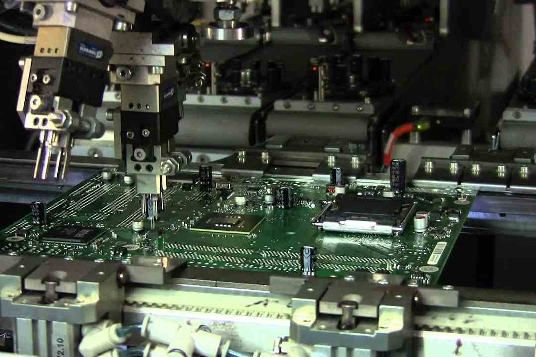
SMT is the most widely used assembly technology in modern PCB manufacturing. ShwayPCB's SMT assembly line is equipped with high - speed pick - and - place machines that can accurately place components with a pitch as small as 0.3 mm. The process starts with the application of solder paste to the PCB pads using a stencil. The components are then placed on the pads, and the board is passed through a reflow oven, where the solder paste melts and forms reliable electrical connections between the components and the PCB.
4.2 Through - Hole Technology (THT) Assembly
For components that require higher mechanical strength or are not suitable for SMT, such as connectors and power transistors, THT assembly is used. ShwayPCB offers both manual and automated THT assembly services. In manual THT assembly, operators insert the components into the drilled holes on the PCB, and then the leads are soldered using a wave soldering machine or by hand - soldering.
4.3 Mixed Technology Assembly
Many modern PCBs use a combination of SMT and THT components. ShwayPCB has the capability to handle mixed - technology assembly projects efficiently. The company optimizes the assembly process to ensure that both SMT and THT components are assembled correctly and reliably, minimizing the risk of defects and ensuring high - quality end - products.
4.4 Quality Control in Assembly
Similar to the manufacturing process, quality control is crucial during PCB assembly. ShwayPCB uses AOI, X - ray inspection, and in - circuit testing (ICT) to detect defects such as misaligned components, solder bridges, and open circuits. The company also performs functional testing on the assembled PCBs to verify that they meet the specified performance requirements. The following graph shows the defect reduction over time in PCB assembly at ShwayPCB due to continuous improvement in quality control measures:
[Insert a line graph here showing the decrease in defect rates over a period of 12 - 24 months, with data points for each month.]
5. Quick Turn PCB Assembly: Meeting Tight Deadlines
In today's fast - paced business environment, time - to - market is critical. ShwayPCB offers Quick Turn PCB Assembly services to help clients meet their tight deadlines. The company can provide prototype assembly within 24 - 48 hours and small - batch production within 5 - 7 days, depending on the complexity of the project.
5.1 Benefits of Quick Turn Services
- Faster Product Development: Allows clients to test and validate their designs quickly, reducing the overall product development cycle.
- Reduced Inventory Costs: Enables clients to order smaller quantities initially, minimizing inventory holding costs and the risk of overproduction.
- Competitive Advantage: Helps clients get their products to market faster, giving them an edge over their competitors.
5.2 Case Study: Quick Turn Assembly for a Consumer Electronics Startup
A consumer electronics startup approached ShwayPCB with a request for quick turn assembly of their new smartwatch prototype. The company was able to complete the assembly within 36 hours, allowing the startup to showcase their product at a major trade show. This early exposure helped the startup secure funding and gain market traction, demonstrating the value of quick turn PCB assembly services.
6. Final Delivery and After - Sales Support
Once the PCBs are assembled and tested, they are carefully packaged and shipped to the client. ShwayPCB offers flexible shipping options to meet the client's requirements, including air freight, sea freight, and express delivery.
In addition to delivery, the company provides comprehensive after - sales support. If the client encounters any issues with the PCBs, ShwayPCB's technical support team is available to assist in troubleshooting and resolving the problems promptly.
7. Conclusion
China's turnkey PCB assembly industry, exemplified by ShwayPCB, offers a comprehensive and efficient solution for electronics manufacturers worldwide. From design collaboration and PCB manufacturing to assembly and quick turn services, Chinese providers deliver high - quality products at competitive prices. By choosing a reliable turnkey PCB assembly partner in China, clients can streamline their production processes, reduce costs, and accelerate their time - to - market, giving them a significant advantage in today's competitive global marketplace.
Contact Email: yuan@shwaypcb.com
Website: https://fr4pcb.tech/