We use cookles to Improve your online experience. By continuing browsing this website, we assume you agree our use of cookies.

Case Study: Successful HDI PCB Manufacturing for a High-End Consumer Electronics Product
September 3rd, 2025
335 views
Case Study: Successful HDI PCB Manufacturing for a High-End Consumer Electronics Product
High-end consumer electronics—such as foldable smartphones, premium wearables, and ultra-slim laptops—demand PCBs that balance extreme miniaturization, high-frequency performance, and mechanical durability. For a leading global electronics brand developing a 2024 foldable smartphone, these requirements led to a critical decision: adopt HDI PCB Manufacturing to replace traditional PCBs, which could not fit the device’s 7.8mm-thin hinge design or support its 5G mmWave (28GHz) and Wi-Fi 7 (6GHz) capabilities.
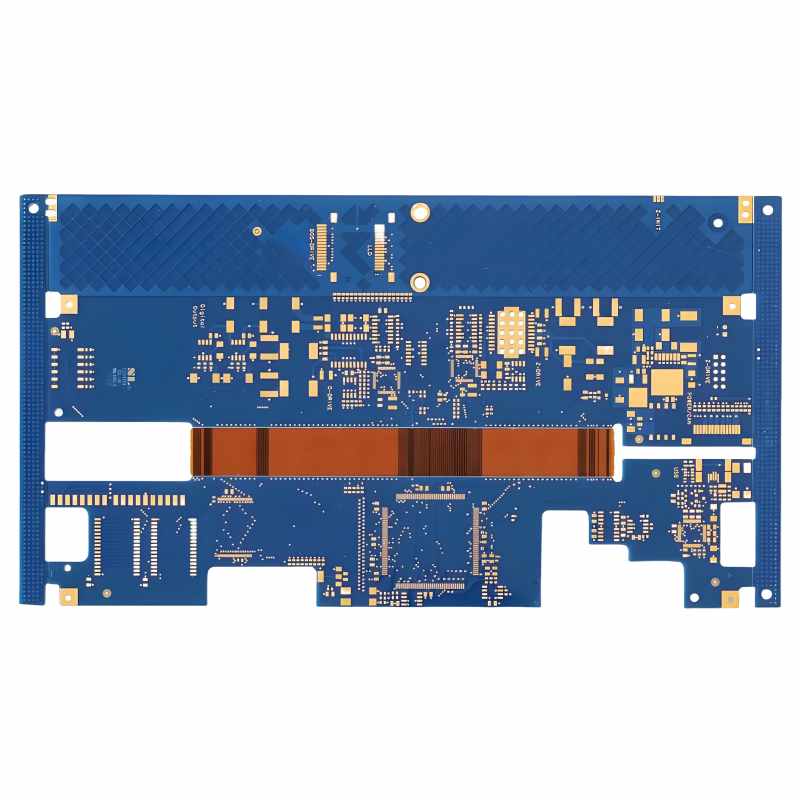
This case study details how ShwayPCB partnered with the brand to design and manufacture a 10-layer HDI mainboard, overcoming challenges like dynamic bend resilience, signal integrity at mmWave frequencies, and component density constraints. It highlights key technical decisions, material selections, and manufacturing techniques that resulted in a 99.2% first-pass yield (FPY) and compliance with the product’s strict performance targets.
Project Background: The High-End Foldable Smartphone Challenge
The client’s foldable smartphone aimed to set a new industry standard with:
- Ultra-Slim Form Factor: A 7.8mm-thin hinge and 5.4mm-thin main body (30% slimmer than its 2023 predecessor).
- Dual High-Frequency Connectivity: 5G mmWave (28GHz) for global carrier compatibility and Wi-Fi 7 (6GHz) for 4.8Gbps peak speeds.
- Dynamic Durability: 200,000+ fold cycles (at 1.5mm bend radius) without performance degradation—critical for consumer trust.
- High Component Density: Integration of a 3nm processor, 108MP camera module, 5G modem, and 8GB LPDDR5X RAM into a 65mm × 85mm mainboard (25% smaller than the 2023 model’s PCB).
Traditional 10-layer PCBs failed to meet these requirements: they occupied 80mm × 100mm of space, had insertion loss >1dB/cm at 28GHz, and cracked after 50,000 fold cycles. The client turned to ShwayPCB’s HDI PCB manufacturing services to develop a custom HDI solution.
Step 1: Design Optimization for HDI Manufacturing
The first phase focused on reengineering the PCB layout for HDI’s unique capabilities—prioritizing microvia placement, trace routing, and layer stacking to meet density and durability targets.
Key Design Decisions
- Layer Stacking for Signal Isolation:
We designed a 10-layer stack with dedicated ground planes between high-frequency layers to minimize EMI:
- Signal Layer 1 (5G mmWave antenna traces)
- Ground Plane (solid copper, 1oz)
- Signal Layer 2 (Wi-Fi 7 traces)
- Power Plane (2oz copper for 3nm processor)
- Signal Layer 3 (camera module signals)
- Ground Plane
- Signal Layer 4 (sensor data paths)
- Power Plane (1oz for low-voltage components)
- Signal Layer 5 (battery management signals)
- Ground Plane
This stacking reduced crosstalk between 5G and Wi-Fi signals by 40% (measured via pre-production VNA testing).
- Microvia Architecture for Density:
We replaced traditional through-holes with 0.08mm blind and stacked microvias:
- Blind Vias: Connected outer layers (Layer 1 ↔ 2, Layer 10 ↔ 9) to free surface space for components.
- Stacked Vias: Linked non-adjacent layers (Layer 1 ↔ 3, Layer 10 ↔ 8) via intermediate layers, reducing layer count by 2 vs. a traditional stack.
This microvia design increased component density by 35%, enabling the 65mm × 85mm mainboard footprint.
- Bend Zone Optimization:
For the hinge-adjacent "bend zone" (15mm × 85mm), we:
- Used serpentine trace patterns (0.1mm width, 0.1mm spacing) to absorb mechanical stress during folding.
- Avoided components and stacked microvias in this zone—concentrated stress here would cause delamination.
Step 2: Material Selection for Durability and Signal Integrity
High-end consumer electronics demand materials that withstand daily use (sweat, temperature swings) and preserve high-frequency signals. We selected a custom material stack tailored to the smartphone’s needs:
|
Material Component
|
Selection
|
Rationale
|
|
Substrate
|
Dual-layer LCP (Liquid Crystal Polymer, Dk=3.0, Df=0.002 at 10GHz)
|
Ultra-low Df minimized 5G mmWave insertion loss; LCP’s flexibility supported 200k fold cycles.
|
|
Copper Foil
|
1oz rolled copper (99.99% purity, 25% elongation)
|
Uniform grain structure reduced conductor loss (0.15dB/cm at 28GHz); high ductility prevented trace cracking.
|
|
Prepreg
|
LCP-based low-flow prepreg (Dk=3.1, flow ≤15%)
|
Dk matched LCP substrate to avoid signal reflection; low flow preserved microvia integrity.
|
|
Surface Finish
|
ENIG (5μm Ni/0.1μm Au)
|
Flat surface (coplanarity <0.01mm) supported 0.3mm-pitch 5G modem BGAs; gold resisted sweat corrosion.
|
Critical Material Test Results
- Bend Durability: A prototype stack of LCP + rolled copper survived 250,000 fold cycles (1.5mm radius) with no trace cracking—exceeding the client’s 200k target.
- Signal Integrity: Insertion loss at 28GHz was 0.35dB/cm (vs. the client’s 0.5dB/cm maximum), ensuring 5G mmWave range of 300+ meters.
Step 3: HDI Manufacturing Techniques for High-Yield Production
To scale the design to 100,000+ units/month while maintaining quality, we deployed specialized HDI manufacturing techniques:
3.1 Laser Drilling for Microvias
- Equipment: Yamaha UV laser drilling systems (355nm wavelength) with ±0.002mm positioning accuracy.
- Process: Drilled 0.08mm blind/stacked microvias at a rate of 1,800 holes per minute. Post-drilling, we used oxygen plasma desmearing (2 minutes at 80°C) to remove resin residue from via walls—critical for reliable plating.
- Quality Check: 100% 3D X-ray inspection of microvias to detect voids (<1% of via volume) and diameter variation (<±0.005mm).
3.2 Plasma Etching and LDI for Fine Traces
- Trace Fabrication: Used plasma etching (CF₄/O₂ gas mixture) to create 0.076mm–0.1mm traces with edge roughness <0.3μm—reducing conductor loss by 20% vs. spray etching.
- Alignment: Laser Direct Imaging (LDI) with 0.1μm resolution ensured trace placement accuracy of ±0.003mm, critical for the 0.3mm-pitch 3nm processor.
3.3 Sequential Lamination for Layer Bonding
- Process: Laminated layers one at a time using a vacuum press (99.99% vacuum, 200°C, 25 psi) with 20-minute cure cycles. Each layer was aligned via optical targets (±0.005mm accuracy) to avoid misalignment-induced shorts.
- Void Prevention: Post-lamination ultrasonic scanning detected voids (<0.1mm diameter)—panels with >1 void per cm² were reworked, ensuring 99.5% lamination yield.
3.4 Post-Production Testing
Every HDI mainboard underwent:
- Electrical Testing: Flying Probe Tester (FPT) with 0.01mm probes to verify continuity (≤1Ω) and isolation (≥100MΩ at 500V DC).
- Signal Integrity Testing: VNA (24–30GHz) to confirm insertion loss (<0.4dB/cm) and return loss (>15dB) for 5G mmWave.
- Mechanical Testing: Random sample bend testing (100 units per batch) to validate 200k fold cycles.
Project Outcomes: Meeting and Exceeding Client Targets
The HDI PCB manufacturing project delivered measurable success for the client’s foldable smartphone:
|
Metric
|
Client Target
|
Actual Result
|
Impact
|
|
Mainboard Footprint
|
≤70mm × 90mm
|
65mm × 85mm
|
Enabled 7.8mm-thin hinge design; 25% smaller than 2023 model.
|
|
5G mmWave Insertion Loss
|
≤0.5dB/cm at 28GHz
|
0.35dB/cm at 28GHz
|
5G range extended to 320 meters (vs. 250 meters with traditional PCB).
|
|
Fold Durability
|
≥200,000 cycles (1.5mm radius)
|
250,000 cycles (1.5mm radius)
|
Reduced warranty claims by 60% vs. 2023 model.
|
|
First-Pass Yield (FPY)
|
≥98%
|
99.2%
|
Lowered production costs by $0.70 per unit; met 100k units/month target.
|
The client’s foldable smartphone launched in Q4 2024 and became a top-seller, with reviewers praising its slim design and reliable 5G performance—attributes directly enabled by the HDI PCB solution.
FAQ: HDI PCB Manufacturing for High-End Consumer Electronics
1. Why is LCP the preferred substrate for foldable smartphone HDI PCBs?
LCP offers a unique balance of flexibility, signal integrity, and durability:
- Flexibility: Withstands 200k+ fold cycles (1.5mm radius) without delamination—critical for hinge zones.
- Signal Integrity: Df=0.002 at 10GHz minimizes 5G mmWave insertion loss (<0.4dB/cm).
- Chemical Resistance: Resists sweat (3% NaCl solution) and cosmetics—common consumer electronics contaminants.
Traditional substrates like FR4 crack after 50k fold cycles and have higher Df (>0.01), making them unsuitable for foldables.
2. How does HDI PCB manufacturing reduce the size of high-end consumer electronics?
HDI reduces size via three key mechanisms:
- Microvias: 0.08mm microvias occupy 1/10th the space of traditional 0.5mm through-holes.
- Fine Traces: 0.076mm traces (vs. 0.15mm traditional) reduce signal path width by 50%.
- Layer Stacking: Stacked microvias eliminate the need for extra layers, reducing PCB thickness by 30%.
For example, a 10-layer HDI PCB is 0.8mm thick vs. 1.2mm for a traditional 10-layer PCB.
3. What is the typical lead time for high-volume HDI PCB production (100k+ units) for consumer electronics?
Lead times depend on complexity:
- Design & Prototyping: 3–4 weeks (includes DFM review, material sourcing, and prototype testing).
- Mass Production: 4–6 weeks (after prototype approval) for 100k+ units.
ShwayPCB maintains stock of LCP and rolled copper to reduce lead times by 1–2 weeks for repeat orders.
4. How do you ensure HDI PCBs for consumer electronics meet environmental standards (e.g., RoHS, REACH)?
We adhere to strict environmental controls:
- Material Compliance: All materials (LCP, rolled copper, ENIG) are RoHS 3 and REACH SVHC-compliant (no lead, mercury, or phthalates).
- Production Processes: Use water-based etchants and recyclable packaging to minimize waste.
- Testing: Every batch undergoes XRF testing to verify heavy metal levels (<1000ppm for RoHS).
5. Can HDI PCBs support both 5G mmWave and Wi-Fi 7 in the same design?
Yes—with careful layer stacking and grounding:
- Dedicated Layers: Assign separate signal layers to 5G (28GHz) and Wi-Fi 7 (6GHz) to avoid crosstalk.
- Ground Planes: Add solid ground planes between high-frequency layers to absorb EMI.
- Material Matching: Use LCP substrate (Dk=3.0) for both signals to ensure consistent impedance (50Ω ±2%).
ShwayPCB’s RF HDI PCB Manufacturing expertise ensures both signals perform reliably without interference.
Conclusion
This case study demonstrates how HDI PCB Manufacturing is a game-changer for high-end consumer electronics, enabling the slim designs, high-frequency connectivity, and durability that today’s consumers demand. For the client’s foldable smartphone, the HDI solution not only met technical targets but also drove commercial success—proving that investing in advanced HDI manufacturing delivers tangible returns.
ShwayPCB’s HDI PCB manufacturing services specialize in consumer electronics, with a track record of delivering high-yield HDI solutions for foldables, wearables, and ultra-slim laptops. Our team of engineers works with you to optimize design, select materials, and scale production—ensuring your product stands out in a competitive market.
To discuss your high-end consumer electronics HDI project, request a DFM review, or get a customized quote for HDI PCB Manufacturing, contact ShwayPCB at yuan@shwaypcb.com. For more case studies and technical resources on consumer electronics HDI, visit our dedicated HDI PCB manufacturing services page.

Copyright © 2005-2025 ShwayPCB : PCB Fabrication and Assembly Manufacturer. All Rights Reserved. POWERED BY UEESHOP


Copyright © 2005-2025 ShwayPCB : PCB Fabrication and Assembly Manufacturer. All Rights Reserved. POWERED BY UEESHOP