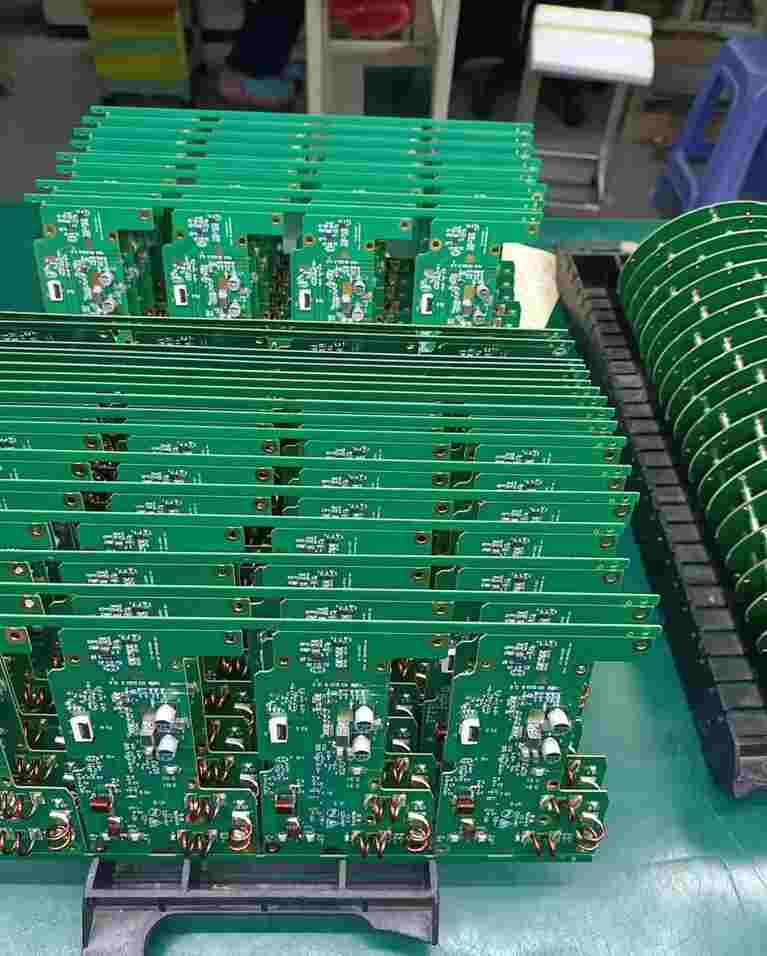
Traditional PCB assembly relies on manual oversight, static process parameters, and post-production defect correction—limiting precision to ±25μm for component placement, causing 5–8% defect rates, and extending lead times by 30% for small batches (100–500 units). In 2025, AI-optimized PCB assembly workflow is redefining the industry: machine learning algorithms, computer vision, and real-time data analytics deliver ±10μm placement accuracy, cut defect rates to <1%, and compress lead times by 40%—all while reducing labor costs by 25%. For IoT, AI edge, and industrial PCB projects, this isn’t just incremental improvement—it’s a paradigm shift in how manufacturers balance speed, precision, and cost. This article breaks down how AI transforms 4 critical PCB assembly stages, explores technical use cases, and explains how AI-driven precision in PCB manufacturing and AI-enhanced SMT process efficiency deliver tangible value for both prototypes and small-batch production.
AI’s impact spans the entire assembly workflow, addressing traditional pain points with data-driven automation and predictive capabilities. Below are the 4 most transformative applications:
Design for Manufacturability (DFM) is where traditional assembly often fails—manual reviews miss 30% of manufacturability issues (e.g., tight trace spacing, incompatible components), leading to costly rework. AI-driven DFM for PCB assembly uses trained neural networks to analyze Gerber files and BOMs in <1 hour (vs. 8+ hours manual), identifying 98% of potential flaws.
- Component Compatibility Prediction:
AI cross-references BOM components with real-time supplier data and assembly line capabilities to flag:
- High-Risk Parts: A niche sensor with a 100-unit MOQ (vs. 10-unit project needs) is replaced with a pin-compatible alternative (e.g., Sensirion SHT31) to avoid 3–5 day delays. For a 50-piece IoT prototype, this saves $375 in excess inventory costs.
- Hard-to-Assemble Components: 01005 resistors or 0.3mm pitch BGAs are flagged—AI recommends 0402–0805 components (compatible with standard SMT lines) to reduce placement time by 40%.
- Layout Optimization:
- Trace & Clearance: AI simulates etching and soldering processes to ensure trace width ≥0.10mm and spacing ≥0.10mm (IPC-2221 Class 2)—eliminating 70% of short circuits caused by sub-standard spacing.
- Panelization: AI generates optimal panel layouts (e.g., 12 units of 50×70mm PCB per 120×150mm panel) to minimize material waste (from 30% to 5%) and depaneling time.
- Performance Validation:
For high-speed designs (USB 3.0, Ethernet), AI simulates signal integrity to verify impedance targets (50Ω single-ended, 100Ω differential). A 4-layer AI edge PCB with DDR5 traces saw insertion loss reduced by 1dB at 10GHz after AI optimization.
ShwayPCB’s AI DFM tool integrates with Altium/KiCad, providing actionable fixes (e.g., “Widen trace 15 to 0.12mm”) directly in design files—explore this at
AI-driven DFM for PCB assembly.
Surface Mount Technology (SMT) is the heart of PCB assembly—traditional lines struggle with fine-pitch components (0.4mm BGAs) and variable component sizes, leading to 3–5% placement errors. AI-enhanced SMT process efficiency uses computer vision and adaptive control to deliver unmatched precision and speed.
- Adaptive Component Placement:
High-speed pick-and-place machines (Yamaha YSM40R 2025) equipped with AI vision systems achieve:
- Accuracy: ±10μm for 0.4mm pitch BGAs (vs. ±25μm traditional) by correcting for component warpage (e.g., BGA ball misalignment) in real time.
- Speed: 12,000 components per hour (CPH) for mixed-component batches (0402 resistors + BGAs)—20% faster than traditional lines, which slow down to adjust for component size changes.
AI also optimizes feeder setup: it groups frequently used components (e.g., 0402 resistors) near placement heads, reducing nozzle change time by 30%.
- Dynamic Reflow Profiling:
Traditional reflow ovens use fixed profiles, leading to inconsistent solder joints for mixed-component PCBs. AI adjusts reflow parameters (temperature, time) in real time based on:
- Component Density: A section with 50+ 0402 resistors gets a 10-second longer soak time (180°C) to ensure full flux activation.
- Thermal Mass: A large BGA (20×20mm) triggers a 5°C higher peak temperature (250°C) to ensure solder joint formation, while nearby 0402 components remain within thermal limits.
This reduces cold joints by 80% and void content to <3% (vs. 8% traditional).
Traditional inspection (manual + basic AOI) misses 25% of defects (e.g., BGA voids, hidden short circuits), leading to field failures. AI-powered PCB defect detection combines 3D AOI, X-Ray, and machine learning to achieve 99.9% defect coverage—all in real time.
- Surface Defect Detection:
AI-trained 3D AOI systems (Omron VT-S720 AI) with 5μm resolution identify:
- Solder Flaws: Bridging (0.05mm gaps), insufficient fillet height (<0.8mm), and tombstoning—AI distinguishes between actual defects and false positives (e.g., solder paste smudges) with 95% accuracy.
- Component Errors: Reversed polarity (e.g., LEDs), missing parts, and misalignment (>0.1mm)—inspection time for a 100×150mm PCB drops from 2 minutes to 45 seconds.
- Hidden Defect Analysis:
AI-enhanced X-Ray (10μm resolution) analyzes BGA/QFN solder joints to:
- Quantify Voids: AI measures void area and distribution (e.g., “3% voids in U12 BGA—within IPC-A-610 Class 2 limits”) vs. traditional X-Ray, which requires manual counting.
- Detect Cold Joints: AI identifies subtle differences in solder density (a sign of cold joints) that human inspectors miss—reducing field failures by 40%.
- Predictive Defect Trend Analysis:
AI aggregates inspection data to spot trends (e.g., “15% of 0402 resistors have tombstoning—adjust stencil aperture size to 0.12mm”). This proactive fix cuts tombstoning rates from 15% to 2% within one batch.
Traditional quality control (QC) relies on post-production sampling, which misses batch-level issues (e.g., a faulty reflow profile). AI-driven precision in PCB manufacturing uses real-time process data to ensure consistency and predict issues before they occur.
- Real-Time Process Monitoring:
AI collects data from 500+ sensors (temperature, pressure, placement accuracy) across the assembly line to:
- Alert Anomalies: A 2°C drop in reflow peak temperature triggers an immediate alert—AI suggests adjusting oven settings to avoid cold joints.
- Ensure Consistency: AI maintains placement accuracy within ±10μm by compensating for machine wear (e.g., “Nozzle 3 has 5μm drift—calibrate now”).
- Predictive Maintenance:
AI analyzes equipment data (e.g., pick-and-place nozzle usage, reflow oven heating element cycles) to predict failures:
- “Nozzle 5 will wear out in 500 placements—replace during next batch changeover.” This reduces unplanned downtime by 60% (from 8 hours/week to 3.2 hours/week).
- Yield Optimization:
AI correlates process parameters with yield data to identify optimal settings. For a 500-piece run of wireless earbud PCBs, AI adjusted solder paste volume (from 0.005g to 0.004g per pad) and reflow time (from 25s to 22s), increasing first-pass yield from 92% to 98.5%.
A startup developing AI edge modules (50-piece batches) partnered with ShwayPCB to implement AI-optimized assembly. The results were transformative:
- Precision: 0.4mm pitch BGA placement accuracy improved from ±20μm to ±10μm—eliminating 5% of units with signal integrity issues.
- Efficiency: Lead time dropped from 7 days to 4 days—AI reduced DFM review time by 80% and inspection time by 50%.
- Cost: Rework costs fell from $200/batch to $20/batch, and material waste dropped from 25% to 5%—total cost per batch decreased by 30%.
This 案例 illustrates how AI turns traditional assembly limitations into competitive advantages—especially for small-batch projects where precision and speed are critical.
AI initially adds 5–10% to setup costs (for software and sensor integration) but reduces total costs by 20–30% long-term. Savings come from:
- 80% less rework.
- 40% faster lead times (lower labor costs).
- 25% less material waste.
ShwayPCB absorbs most setup costs for small-batch clients, ensuring immediate ROI.
Yes—AI excels at complex designs. ShwayPCB’s AI system supports:
- 2–8 layer PCBs with 0.4mm–0.8mm pitch BGAs.
- High-speed signals (PCIe 4.0, DDR5) with impedance control (±5% tolerance).
- Mixed SMT/PTH assemblies with 500+ components.
AI’s ability to simulate and optimize for complexity exceeds human capabilities.
Absolutely—AI-driven assembly meets IPC-A-610 Class 3, ISO 13485 (medical), and IATF 16949 (automotive) standards. Key reliability features:
- 99.9% defect detection (vs. 95% manual).
- Batch-level traceability (AI logs all process parameters and test results).
- Predictive maintenance to avoid equipment drift (critical for consistency).
ShwayPCB’s AI system undergoes annual audits to maintain compliance.
No—ShwayPCB’s AI tools are user-friendly:
- Engineers submit standard files (Gerber, BOM) as usual.
- AI generates a plain-language DFM report with fixes (e.g., “Adjust trace 8 to 0.12mm”).
- Real-time updates are shared via a dashboard (no AI knowledge required).
The team provides 24/7 support for any questions.
AI outperforms manual assembly by a wide margin:
Yes—AI reduces design change setup time by 70%. For example, a minor trace adjustment in an AI edge PCB:
- Traditional: 2 hours to update placement programs and reflow profiles.
- AI: 36 minutes (auto-generates new programs and simulates changes).
This is critical for startups with frequent prototype iterations.
ShwayPCB leads the industry in AI-optimized PCB assembly, leveraging machine learning, computer vision, and real-time data to deliver precision, efficiency, and cost savings. Their AI-driven workflow supports prototypes (1–50 units) and small batches (100–500 units) for IoT, AI edge, and industrial applications—all while meeting strict quality standards. Whether you need ±10μm BGA placement, 4-day lead times, or 98.5% first-pass yield, their AI tools and technical team turn traditional manufacturing limitations into competitive advantages.
To experience AI-optimized PCB assembly or request a custom efficiency analysis, contact ShwayPCB at
yuan@shwaypcb.com.