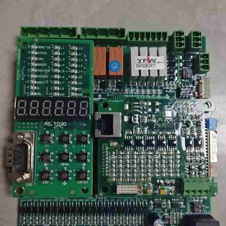
Automated Optical Inspection (AOI) is a cornerstone of quality control in PCB assembly service, detecting surface defects like solder bridging, tombstoning, and component misalignment with speeds 10x faster than manual inspection. However, high false positive rates—often 5–15% in unoptimized programs—create critical bottlenecks: engineers waste hours verifying “defects” that are actually normal variations (e.g., solder paste unevenness, component marking variations). For a High-Reliability PCB Assembly Service, reducing AOI false positives to <1% is not just a efficiency goal—it is essential to maintaining consistent quality and on-time delivery.
ShwayPCB’s
specialized PCB assembly service has optimized AOI programs for 2,200+ clients, achieving <0.8% false positive rates and 99.7% defect detection accuracy. Below, we break down the technical strategies to optimize AOI programs, from lighting setup to AI algorithm training.
Before diving into optimization, it is critical to quantify the impact of high false positive rates on PCB assembly service:
- Rework Time Waste: A 10% false positive rate for a 10k-unit batch means 1,000 boards are incorrectly flagged—each requiring 5–10 minutes of manual verification, totaling 83–167 hours of wasted labor.
- Production Delays: Bottlenecks at the AOI station can slow line throughput by 20–30%, missing client deadlines (e.g., a 48-hour quickturn order delayed by 12 hours due to false positive reviews).
- Quality Risk: Over time, engineers may “tune out” frequent false positives, increasing the risk of missing real defects (e.g., a solder bridge mistaken for a false positive).
These costs make AOI optimization a high-priority for Quickturn PCB Assembly Service and High-Density SMT PCB Assembly Service, where speed and accuracy are non-negotiable.
Reducing false positives to <1% requires a holistic approach addressing lighting, algorithm parameters, component libraries, and data validation. Below are 5 technical strategies:
AOI relies on consistent, targeted lighting to distinguish defects from normal variations—poor lighting is responsible for 30–40% of false positives. High-Precision SMT PCB Assembly Service uses these calibration techniques:
- Multi-Angle Lighting Setup:
- Use 45° angled lights for solder joint inspection (highlights fillet shape and voids).
- Use coaxial lights for component marking verification (reduces glare on glossy surfaces).
- Avoid overhead-only lighting (creates shadows that mimic component misalignment).
- Example: A client’s 01005 resistor inspection had 8% false positives due to shadowing—adding 45° side lights reduced false positives to 1.2%.
- Light Intensity and Exposure Tuning:
- Match intensity to component color (e.g., 60% intensity for dark ceramic resistors, 80% for bright aluminum capacitors).
- Adjust exposure time (10–20ms) to avoid overexposure (washes out small defects) or underexposure (creates noise).
- Tool: Use AOI software’s “histogram analysis” to ensure 80% of pixels fall within the mid-tone range (avoid clipping bright/dark areas).
AOI algorithms use threshold parameters to classify defects—overly strict settings flag normal variations as defects, while loose settings miss real issues. Defect-Free PCB Assembly Service tunes these key parameters:
- Solder Paste Inspection (SPI) Parameters:
- Volume Tolerance: Set to ±15% (not ±5%) for 01005 components (small paste variations are normal).
- Height Uniformity: Allow ±20% variation for BGAs (paste settles unevenly on large pads).
- Bridging Threshold: Ignore gaps <0.05mm for 0.3mm-pitch components (paste “bleed” is non-conductive).
- Component Placement Parameters:
- X/Y Offset: Set to ±0.1mm for 0402 components (vs. ±0.05mm) to account for minor pick-and-place variations.
- Rotation Tolerance: Allow ±2° for passives (vs. ±1°)—rotation has no functional impact for non-polar components.
- Verification: Test tuned parameters on 500+ “good” boards—adjust if false positives exceed 1%.
Case Study: A client’s 0.4mm-pitch BGA inspection had 12% false positives due to strict height uniformity (±5%). Relaxing to ±20% reduced false positives to 0.9% without missing any real defects.
False positives often stem from generic component libraries that fail to account for manufacturer-specific variations (e.g., slightly different resistor sizes, inconsistent marking fonts). Mixed-Technology SMT-DIP PCB Assembly Service builds custom libraries:
- Capture Reference Images:
- Take 5–10 images of each component (from different production lots) to capture variation.
- Include “edge cases” (e.g., components with faint markings, minor lead bending).
- Train Library with Tolerances:
- Set size tolerances to ±5% (matches IPC component size standards).
- Use “pattern matching” (not exact pixel matching) for markings—tolerate 20% variation in font thickness or position.
- Update Libraries Regularly:
- Refresh libraries when switching component suppliers or batches.
Impact: A client’s resistor inspection had 7% false positives due to generic library mismatch—building a custom library reduced false positives to 0.7%.
Modern AOI systems use machine learning to distinguish real defects from false positives—High-Reliability PCB Assembly Service leverages this by:
- Labeling False Positives:
- Manually tag 1,000+ false positives (e.g., “normal paste variation,” “component marking fade”) in the AOI software.
- Train the AI model on these labels (use 80% for training, 20% for validation).
- Continuous Learning:
- Schedule weekly model retraining with new false positive data.
- Set a “confidence threshold” of 85%—only flag defects with >85% confidence for manual review.
Result: ShwayPCB’s AI-optimized AOI reduced false positives from 9% to 0.6% for a client’s 5G PCB assembly, cutting manual review time by 85%.
Optimization is an ongoing process—PCB assembly service must validate AOI results and refine programs:
- Cross-Verify with X-Ray/Manual Inspection:
- For every false positive, check if the AOI missed a real defect (e.g., a “false positive” solder bridge that is actually a micro-bridge).
- Use X-ray to confirm internal defects (e.g., BGA voids) that AOI may misclassify.
- Track Metrics Weekly:
- Monitor false positive rate, defect detection rate, and manual review time.
- Adjust parameters if false positives exceed 1% (e.g., relax a strict offset threshold).
Different PCB designs require tailored AOI optimization—below are guidelines for common use cases in PCB assembly service:
- Use 5MP+ cameras (vs. 2MP) for higher resolution.
- Enable “sub-pixel analysis” to detect small variations (e.g., 0.01mm paste height differences).
- Avoid over-inspecting non-critical areas (e.g., ignore minor paste variation on non-signal pads).
- Use separate AOI programs for SMT (fine-pitch) and THT (large components) areas.
- For THT components, focus on solder fillet shape (not minor lead misalignment).
- Use “region masking” to ignore THT solder flux residue (common and non-conductive).
- Reduce lighting intensity (flexible substrates reflect light unevenly).
- Allow higher offset tolerance (±0.15mm) for components on curved areas.
- Use “warpage compensation” to correct for PCB bending during inspection.
Yes—with a combination of lighting calibration, AI training, and custom libraries. ShwayPCB achieves 0.6–0.9% false positive rates for 0.3mm-pitch BGA PCBs by optimizing all 5 strategies outlined above.
- Standard PCBs (0402, 0.5mm-pitch BGAs): 1–2 days (lighting + parameter tuning).
- High-Density PCBs (01005, 0.3mm-pitch BGAs): 3–5 days (includes AI training and library building).
- Quickturn projects: ShwayPCB offers expedited optimization (24–48 hours) for Quickturn PCB Assembly Service.
No—most existing AOI systems (5+ years old) support lighting calibration, parameter tuning, and basic AI training. For systems >10 years old, upgrading software (not hardware) can enable AI features, costing $5k–$15k vs. $100k+ for new equipment.
Optimization improves detection rates by reducing “noise” from false positives—engineers focus on real defects instead of verifying false alarms. ShwayPCB’s clients see a 5–10% increase in defect detection after optimization.
For a 10k-unit monthly batch with 10% false positives:
- Before optimization: 1,000 false positives × 10 minutes review = 167 hours wasted labor ($8,350 at $50/hour).
- After optimization (1% false positives): 100 false positives × 10 minutes = 17 hours ($850).
- Monthly savings: $7,500—ROI is typically achieved in 1–2 months.
AOI program optimization is a high-impact, low-cost way to reduce false positives to <1% in PCB assembly service, cutting rework time, eliminating delays, and improving quality. By combining lighting calibration, algorithm tuning, custom libraries, AI training, and continuous validation, manufacturers can unlock the full potential of AOI as a quality control tool.
ShwayPCB’s
specialized PCB assembly service offers end-to-end AOI optimization, including
High-Precision SMT PCB Assembly Service,
High-Reliability PCB Assembly Service, and
Quickturn PCB Assembly Service. Our team of AOI experts provides program tuning, AI model training, and ongoing support to ensure your AOI system operates at peak efficiency.
To request an AOI optimization assessment, access our parameter tuning checklist, or get a quote for specialized PCB assembly, contact ShwayPCB at
yuan@shwaypcb.com. For detailed AOI case studies (automotive, medical, 5G), visit our
specialized assembly service page.